|
|
16-bit demultiplexer / 8-bit demultiplexer |
| 1. Specifications | Planning | Developing | Testing | Report | Prototype |
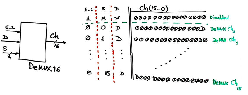
Design a DeMUX_16 similar to the classic 74HCT154 chip in a programmable logic device (PLD) target chip.The circuit symbol and its truth table is represented in Fig. 1.
 |
|
Fig. 1. DeMUX_16 symbol and truth table. Select channel input S(3..0) and outptus Ch(15..0) are defined as vectors. |
As an initial theory review, explain what kind of applications will use DeMUX, and what may be input data D.
| Specifications | 2. Planning | Developing | Testing | Report | Prototype |
Plan B capturing in VHDL the truth table or proposing the circuit algorithm as a flowchart.
An example schematic and VHDL translation is used in lecture L2.2. Complete your schematic in your plan sheet before translating it to VHDL.
The project location may be:
C:\CSD\P2\DeMUX_16B\(files)
Plan C2 hierarchical circuit using DeMUX_8 components. The project location may be:
C:\CSD\P2\DeMUX_16C2\(files)
| Specifications | Planning | 3. Developing | Testing | Report | Prototype |
An example schematic and VHDL translation is used in lecture L2.2. This is a VHDL translation DeMUX_16.vhd.
| Specifications | Planning | Developing | 4. Testing | Report | Prototype |
We can run a testbench applying some stimulus to see whether our circuit works. Prepare a testbench fixture in paper and use Quartus Prime to generate the skeleton. Add the stimulus process. Use ModelSim to test it and obtain waveforms. It is going to be the same testbench file for all DeMUX_16 architectures describing the same entity.
| Specifications | Planning | Developing | Testing | 5. Report | Prototype |
Follow this rubric for writing reports.
|
16-bit demultiplexer / 8-bit demultiplexer |
| 1. Specifications | Planning | Developing | Testing | Report | Prototype |
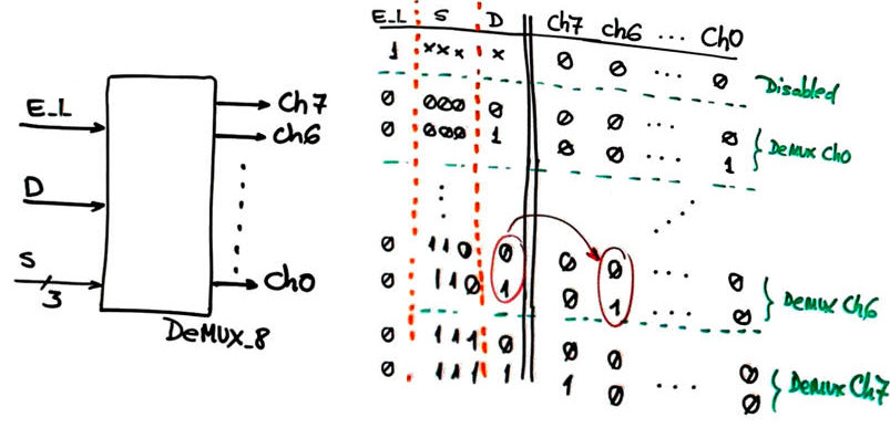
Design a DeMUX_8 similar to the classic 74HCT138 chip in a programmable logic device (PLD) target chip. The circuit symbol and its truth table is represented in Fig. 1. Use plan A equations.
 |
|
Fig. 1. DeMUX_8 symbol and truth table. Select channel input S(2..0) is defined as vector. All other inputs and outputs are individual wires. |
| Specifications | 2. Planning | Developing | Testing | Report | Prototype |
Plan A using our VHDL design flow using logic equations and EDA tools for developing and testing.
Example equations are used in lecture L2.2. The project location may be:
C:\CSD\P2\DeMUX_8A\(files)
Plan C2 hiearchical circuit using DeMUX_4 components. The project location may be:
C:\CSD\P2\DeMUX_8C2\(files)
| Specifications | Planning | 3. Developing | Testing | Report | Prototype |
An example schematic and VHDL translation is used in lecture L2.2.
| Specifications | Planning | Developing | 4. Testing | Report | Prototype |
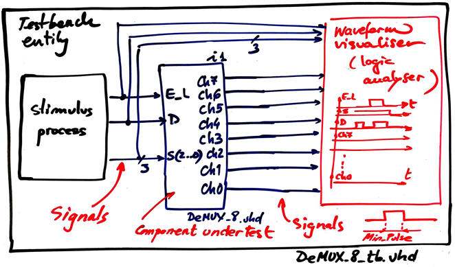
We can run a testbench applying some stimulus to see whether our circuit works. Prepare a testbench fixture in paper as shwon in Fig. 2 and use Quartus Prime to generate the skeleton. Add the stimulus process. Use ModelSim to test it and obtain waveforms. It is going to be the same testbench file for all DeMUX_8 architectures describing the same entity.
 |
| Fig. 2. Testbench fixture for testing the designed entity. |
Use a VHDL testbench (DeMUX_8_tb.vhd file) in ModelSim to verify that the demultiplexer works as expected in Fig. 3.
 |
| Fig. 7. Timing diagram demonstrating how the circuit works. |
| Specifications | Planning | Developing | Testing | 5. Report | Prototype |
Follow this rubric for writing reports.
| Specifications | Planning | Developing | Testing | Report | 6. Prototype |
A MUX-DeMUX circuit for experimentation is explained in LAB2.