|
|
Bachelor's Degree in Telecommunications Systems and in Network Engineering |
|
P2: Standard logic circuits: multiplexer, decoder, etc. Plan A, plan B: flat single-file VHDL architecture |
| Resources in lectures and labs: | L2.1, Lab2, L2.2, L2.3, L2.4, L2.5 | Project | objectives |
Highlighted project: Hexadecimal to 7-segment decoder (type 74LS47) using plan A
| 1. Specifications | Planning | Developing | Testing | Report | Prototype |
Design HEX_7seg_decoder similar to the standard chip 74LS47 using plan A, for instance, sums of products (SoP) or products of sums (PoS) equations.
Draw the circuit's symbol, truth table and an example of timing diagram.
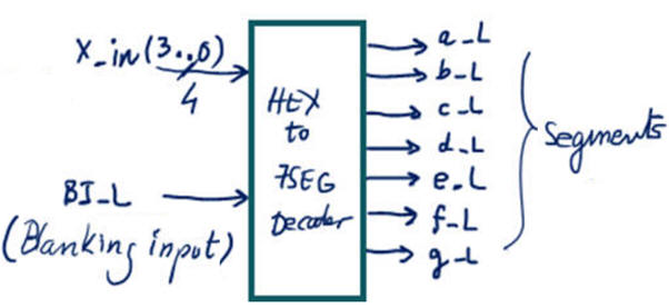 |
| Fig. 1. Hexadecimal to 7-segment decoder. A similar standard chip is the 74LS47. |
When blanking input active-low (BI_L) is active with '0', all outputs are high ('1'), meaning that no LED is lighting (blanked).
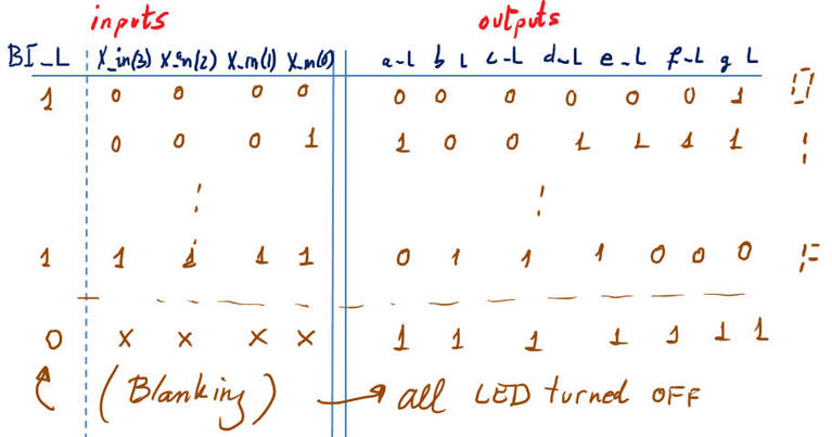 |
| Fig. 2. This is the truth table to define how the circuit works, and that always goes attached to the symbol. |
Example of a timing diagram. Draw some input vectors and figure out what are going to be the outputs. Using vertical time cursors identify the minimum time in which signals are stable, this is our Min_Pulse constant to which refer all time values.
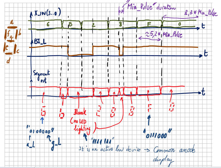 |
| Fig. 3. Sketch of timing diagram for this circuit. |
Fig. 4 represents a similar circuit Dec_hex_7seg.pdsprj with additional control signals captured for running in Proteus simulator.
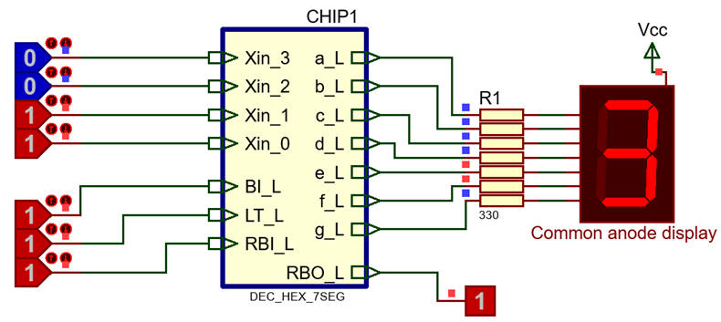 |
| Fig. 4. A hexadecimal to 7-segment decoder in Proteus. |
Optional additional feature: Add ripple blanking input RBI_L and ripple blanking output RBO_L functionality to our circuit to be able to chain decoders for blanking leading zeroes.
This is another Proteus circuit where to study the mechanism of the input-output ripple blanking chain to blank leading zeroes when multiple displays are used. For instance, in a 10-digit calculator, a given result such "0000010345" is better represented as: " 10345" where all leading zeroes are blanked.
|
|
Other design tutorials and assignments. Precisely, the project Hex_7seg_decoder is the same circuit using plan B, thus you can compare both internal architectures.
| Specifications | 2. Planning | Developing | Testing | Report | Prototype |
VHDL design flowchart. Fig. 5. may be a sequence of operations for inventing HEX_7seg_decoder in a single-file VHDL project using plan A.
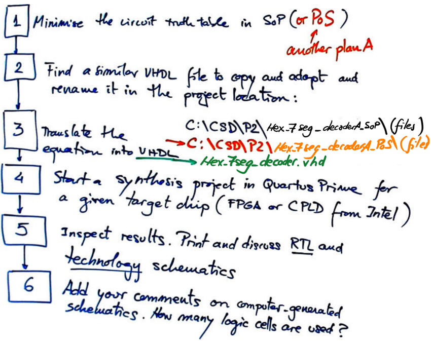 |
| Fig. 5. Planning the development (synthesis) of the circuit. |
Project location (remember to change your project location if you have a different set of equations):
C:\CSD\P2\HEX_7seg_decoderA_SoP\(files)
The verification of the circuit under test may be carried out following Fig. 6 sequence.
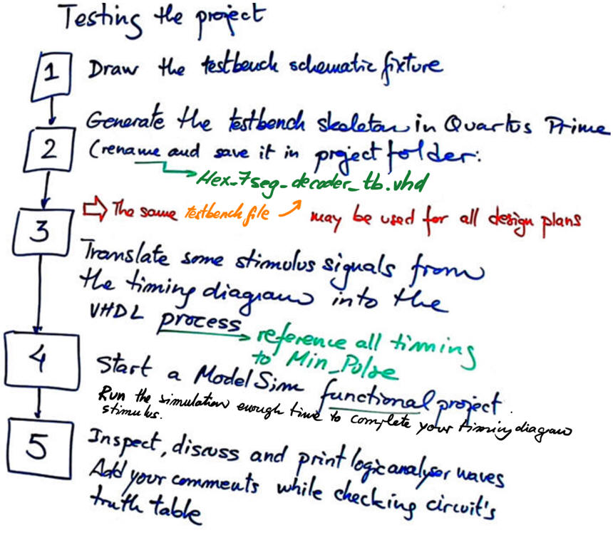 |
| Fig. 6. Testing procedure. |
| Specifications | Planning | 3. Developing | Testing | Report | Prototype |
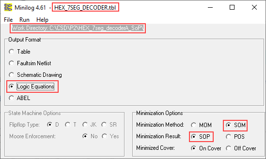
Write the table format file to be used as the truth table input for Minilog.exe, for example HEX_7seg_decoder.tbl file.
Use SoP (or alternatively PoS) to obtain the minimised equations from the truth table.
 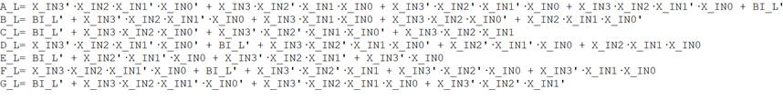 |
| Fig. 7. List of minimised equations in SoP format. |
Find a similar VHDL file described using equations and rename it. Edit the file to translate circuit equations into VHDL, for example: hex_7seg_decoder.vhd.
Start an EDA project for a CPLD/FPGA chip (HEX_7seg_decoder_prj) and obtain the synthesised circuit. For instance select MAX 10 FPGA 10M50DAF484C7.
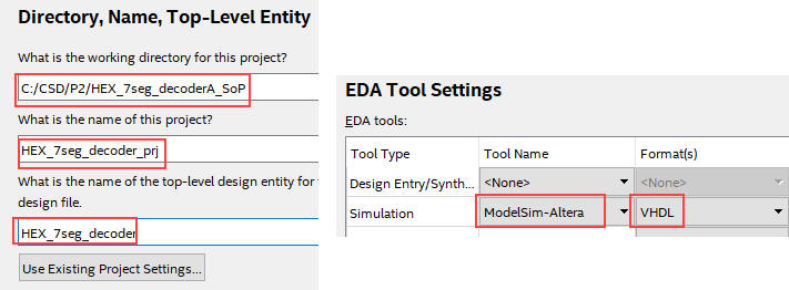 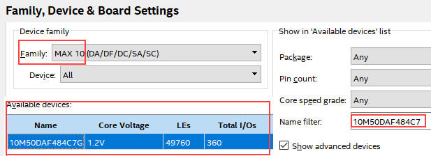 |
Fig. 8. Quartus Prime parameters. Intel chip MAX10 10M50DAF484C7 contains around 50.000 logic elements and 360 bidirectional I/O pins. |
Represent and analyse the RTL and technology views. Fig. 9 is an example of RTL view schematic synthesised by the computer tool.
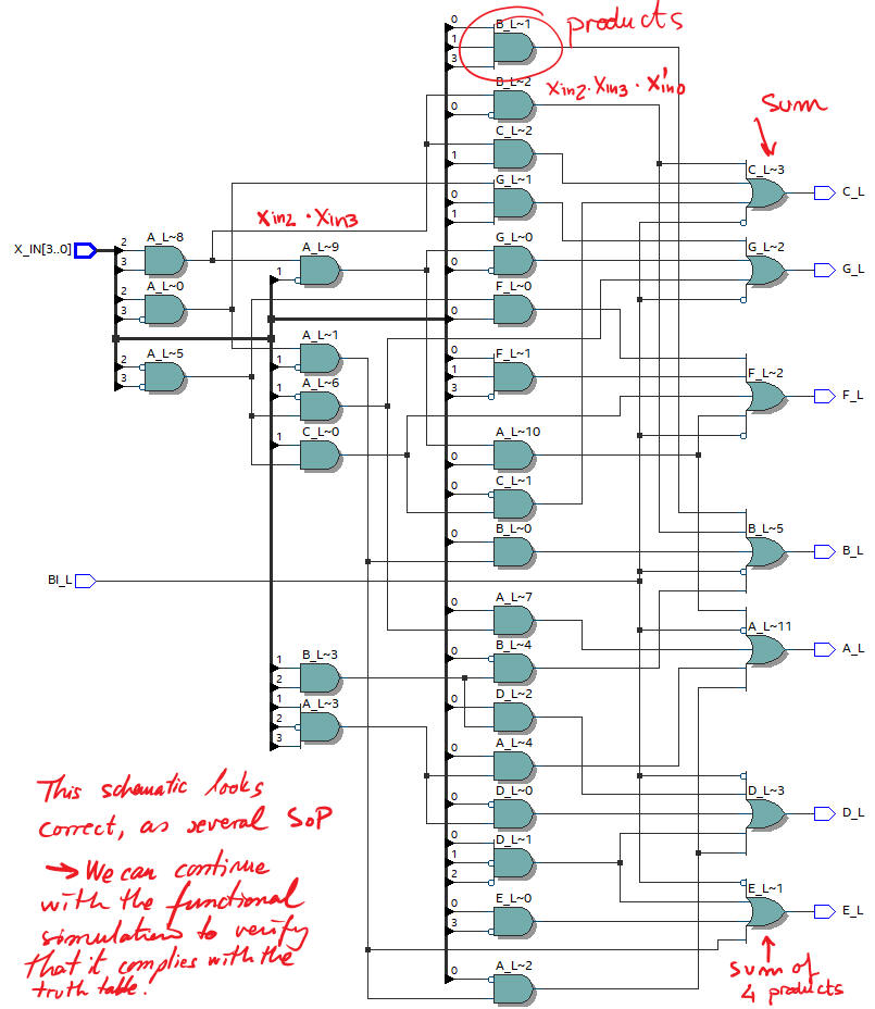 |
| Fig. 9. RTL view. This is the "ideal circuit" pretty much as the way it is described by SoP equations but using 2-input and 3-input AND gates for composing products. |
We can discuss how it is implemented in technology in Fig. 10. How many chip resources are used (logic elements)?
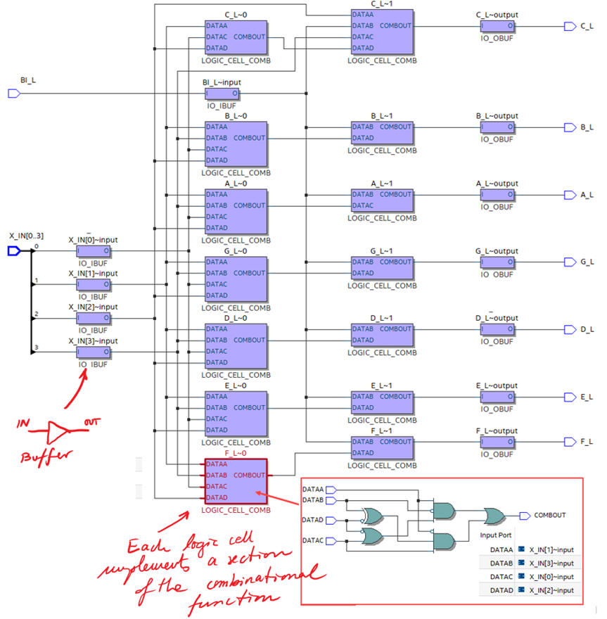 |
| Fig. 10. Printing the technology schematic, the internal structure of which is chip dependent. |
| Specifications | Planning | Developing | 4. Testing | Report | Prototype |
The idea of testbench for circuit verification is represented in Fig. 11.
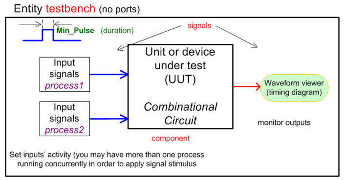 |
| Fig. 11. Diagram representing the concepts associated with a test bench. |
Fig. 12 shows how to generate automatically a testbench skeleton template in Quartus Prime.
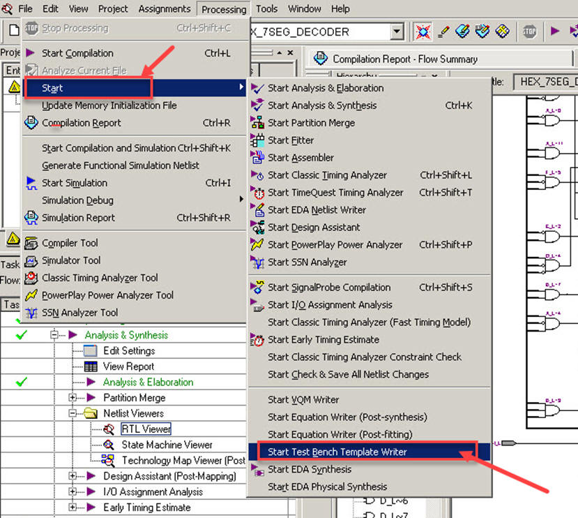 |
| Fig. 12. Generating the testbench template. |
This is an example file HEX_7SEG_decoder_tb.vhd where some stimulus inputs from Fig. 4 are placed in a process.
Start an EDA VHDL simulator project in ModelSim Starter Intel Edition (or ActiveHDL Lattice Edition or Xilinx ISim), and verify the device/unit - under - test (DUT/UUT) using our VHDL simulator test bench.
Print an example of timing diagram screen and add comments on the signals to show how the device works.
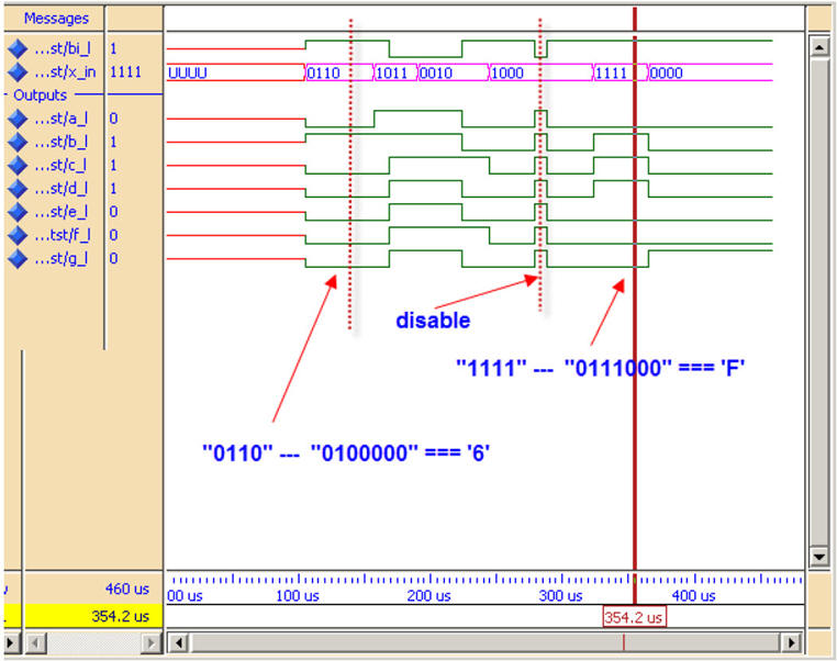 |
| Fig. 13. Functional simulation. |
| Specifications | Planning | Developing | Testing | 5. Report | Prototype |
Follow this rubric for writing reports.
| Specifications | Planning | Developing | Testing | Report | 6. Prototype |
We can use the DE10-Lite board to implement this project, as shown in DE10-Lite tutorial unit. Study the user manual and generate a HEX_7seg_decoder_top schematic to assign input and output pins.
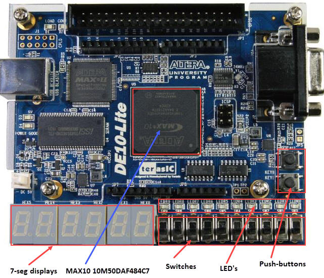 |
Fig. 14. Terasic DE10-Lite board is populated with Intel chip MAX10 10M50DAF484C7 that contains around 50000 logic elements and 360 bidirectional I/O pins |
|
|
Annex: Testing the design using Proteus model for sPLD 22V10 and Lattice tools
Another version of the same project synthesised using Lattice Semiconductor EDA tools ispLEVER Classic.
1. This is the Proteus project Hex_7seg_decoder.pdsprj that contains the simple programmable logic device (SPLD) AM22V10. Save it in project folder:
C:\CSD\P2\Hex_7seg_decoder_A_sPLD\(files)
2. The circuit pdsprj and the sPLD configuration file hex_7seg_prj.jed have to be placed in the same folder. The sPLD configuration jed file is obtained completing the VHDL synthesis flow describing the Hex_7seg_decoder.vhd using VHDL language and running an EDA tool such as Lattice ispLEVER Classic. A license is required to use this propietary software. This is an example report file to see equations and pin assignments to input and output ports.
3. Attach the *.jed file to the AM22V10 sPLD in the Proteus schematic and run a simulation to obtain the truth table and verify that the circuit works as expected, as if it had been designed using classic technologies.
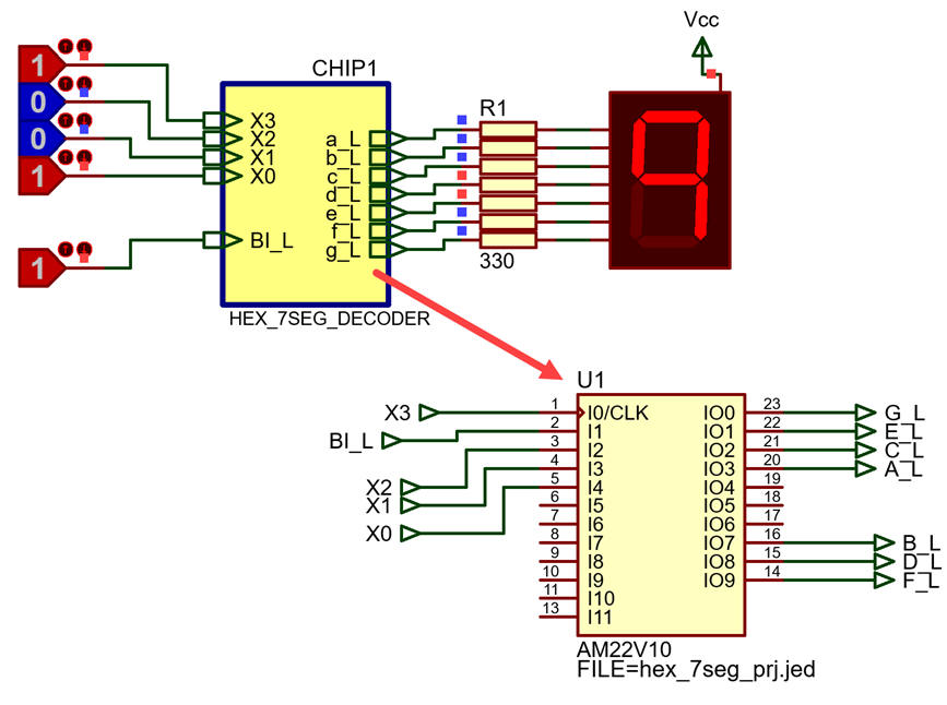 |
| Fig. 13. Simulation of the HEX_7seg_decoder implemented in a sPLD device GAL22V10. |
| Home Term 24/25-Q1 Contact Products Electronic devices and companies Software Books Magazines Instruments DEE Library EETAC DEEL |

|
|
| Web activa des de 09/2001, @ F. J. Robert, J. Jordana. Web editat amb Microsoft Expression Web 4. El contingut és un complement als materials d'estudi del curs Circuits i Sistemes Digitals disponibles al campus digital Atenea. Llicència:Reconeixement 4.0 Internacional de Creative Commons |