|
|
Bachelor's Degree in Telecommunications Systems and in Network Engineering |
|
|
|
|||||
Chapter 2 problems |
- D2.6 - |
7-segment digit sequencer (FPGA-VHDL) |
|||
|
|
|||||
1. Specifications
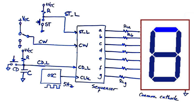
We want to design a driver to show a sequence of movement, clockwise and counter-clockwise, in a single 7-segment display. Fig. 1 represents the schematic diagram of the application. CLK signal to move segments is a 5 Hz rectangular wave. There is a switch to configure movement direction: CW = '1', clockwise; CW = '0' counter-clockwise.
The same project designed programming a μC is in D3.6.
 a) a)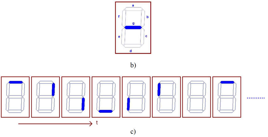 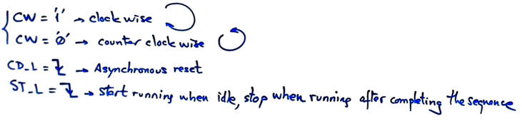 |
|
Fig. 1. a) Circuit schematic. b) Digit segments and position when idle. c) Sequence of switching LED segments for CW = '1' clockwise or up-counting. |
Fig. 1c shows the sequence of segment lighting when CW = '1'. When the system remains idle, the only segment lighting continuously is g.
When clicking the push-button start/stop ST_L the system runs continuously in the configured direction.
When running, if ST_L is clicked again, the system stops after completing the sequence.
2. Planning
A commercial product has to be organised planning several design phases.
Design phase #1: basic features.
Solve the circuit for the design step #1. Only when it is fully tested working correctly and reported, solve the design step #2.
Design step #1. Consider an initial circuit with no CW input, thus representing only clockwise movement.
Design step #2. Add the CW switch.
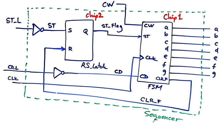
Let us start with the design step #1. Because of the requirement that the sequence must end only when completed after detecting an ST_L falling edge, we need a 1-bit memory cell to save this event when occurs, for instance an RS_Latch. When running, the FSM will generate the sequence as if it were counting in one-hot, one LED segment at a time. Therefore, this is a plan C2 system composed of a top design (sequencer) and some components.
Some questions to kick off the project.
Infer a circuit for solving this project. Fig 2 shows an initial example of internal design using two components. Once used (acknowledged), the ST_Flag has to be reset, thus, the FSM has to generate as well the internal signal CLR_F for the RS_Latch.
 |
|
Fig. 2. First idea of the Sequencer circuit internal architecture. CW switch is only to be considered for the design step #2. |
Firstly we will design the FSM chip, secondly we can proceed with the other components.
FSM
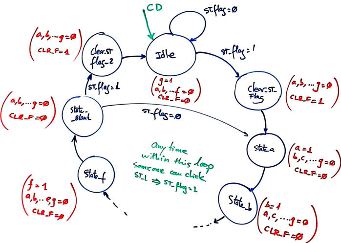
Imagine how the FSM circuit will work. Infer how many resources the circuit may contain and try to draw a state diagram for the circuit's FSM as shown in Fig. 3.
 |
|
Fig. 3. Idea of state diagram for this application. |
To see whether this proposed circuit and state diagram may work correctly, we can draw some waveforms in a timing diagram as in Fig. 4.
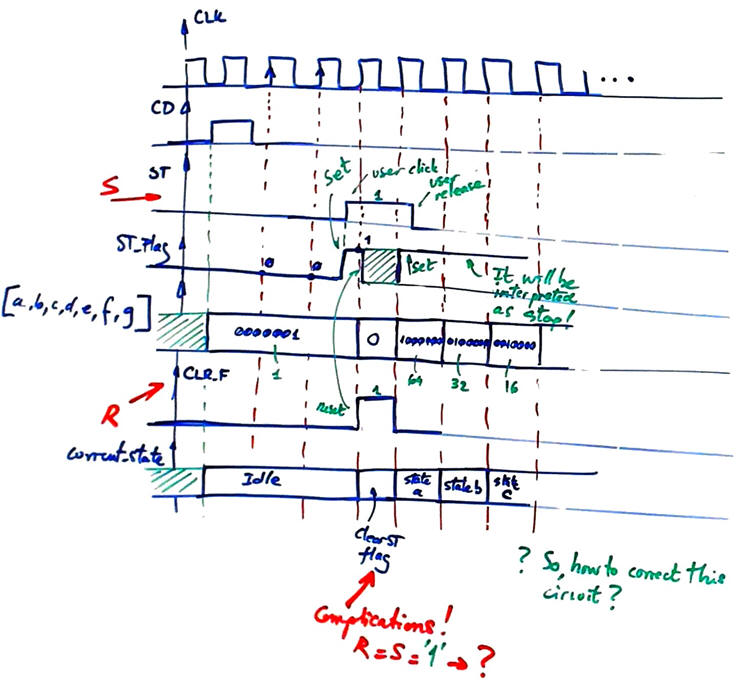 |
| Fig. 4. Example timing diagram when clicking ST one time. Analysing the waveforms for a short click we see that the circuit presents complications because RS_latch inputs R = S = '1' for a while, generating an undefined signal that cannot be used as input by the FSM. |
Therefore, it is not clear that the circuit works as stated. How can we solve these complications driving correctly the RS_Latch? Can you solve the problem modifying the state diagram or the circuit?
The duration of the click depends on the user. We can have short clicks (TCLICK < 2 TCLK) and also long clicks (TCLICK > 2 TCLK). For example, the next analysis in Fig. 5 shows how a short click works correctly replacing the RS_latch by an RS_FF. However, a long user click invalidates the ST_Flag signal because R = S = '1' is still possible.
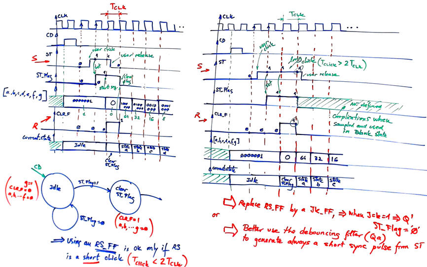 |
| Fig. 4. Analysis of a short and long click. |
Therefore, we can use a JK_FF as the Chip2 in Fig. 2. And we can continue the project in two ways:
(1) Imagining that the user generates always short pulses.
(2) Later, in new design steps, we can introduce extra hardware as Chip3 such the debouncing circuit to generate a single synchronous pulse when clicking (output Qa). In this way, ST will be always a short pulse.
Apply the FSM architecture to this problem.
Deduce how many D_FF are required when encoding FSM states using the following options and draw the state register memory:
Option #1: radix-2 (sequential)
Option #2: Gray
Option #3: Johnson
Option #4: one-hot
Draw the state register based on D_FF considering your state encoding option.
Write the truth table of CC2 and CC1 and their equivalent behavioural interpretations (plan B) using flowcharts.
Project location:
C:\CSD\P6\sequencer\(files)
Write the FSM VHDL file.
Start a Quartus Prime synthesis project for one of the following programmable target chips:
Option #1: Cyclone IV EP4CE115F29C7
Option #2: MAX II EPM2210F324C3
Inspect and annotate the RTL and technology views. Check the number of D_FF synthesised in this application.
Sequencer
Design the RS_Latch component using gates as in L5.1 or using SD and CD in a JK_FF or T_FF disabling the synchronous inputs with CLK = J = K = '0'.
Prepare a VHDL testbench fixture to adapt the stimulus signals in the Fig. 5 sketch. Rely on the constant CLK_Period for setting the time scale.
 |
|
Fig. 5. Testbench fixture. What inputs, outputs and internal signals are to be monitored? |
Run functional simulations to verify your design. Visualise as well in the wave timing diagram the internal states.
Measure the propagation time CLK to output (tCO)using gate-level simulations.
What may be a good estimation of the maximum frequency of operation? Explain your answer.
Design phase #2: Additional features to enhance the product such crystal oscillator for CLK signals nd timers for saving energy when the product is not used.
- Design step #1: Design a CLK generator to obtain the 5 Hz square wave from a 50 MHz quartz crystal oscillator like the one available in the DE10-Lite board. Deduce the number of D_FF that the Sequencer will contain.
- Design step #2: Add a Timer block so that after 2 minutes in Idle state, the system goes to a new Blank_sleep state to save energy, a kind of sleep mode. Clicking ST_L resumes operations.
- Design step #3: Modify the circuit adding a new input button PP (Play/Pause) that when clicked toggles the display. When in play mode, segments work as usual. When in pause, segments a-b-c-d-e -f blinks intermittently at 8 Hz.
| Home Term 23/24-Q2 Contact Products Electronic devices and companies Software Books Magazines Instruments DEE Library EETAC DEEL |

|
|
| Web activa des de 09/2001, @ F. J. Robert, J. Jordana. Web editat amb Microsoft Expression Web 4. El contingut és un complement als materials d'estudi del curs Circuits i Sistemes Digitals disponibles al campus digital Atenea. Llicència:Reconeixement 4.0 Internacional de Creative Commons |