|
|
Bachelor's Degree in Telecommunications Systems and in Network Engineering |
|
|
|
|||||
Chapter 2 problems |
- D2.9 - |
Water tank controller (FPGA-VHDL) |
|||
|
|
|||||
1. Specifications
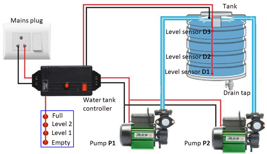
We want to design a water tank controller (Water_tank_controller) as an FSM that can drive two pumps independently, as represented in Fig. 1. The tank has level sensors D1, D2, and D3 attached to the wall, so that a '1' is generated when the sensor is sunk into water. The controller works as follows: when the tank is empty, below D1, both pumps work simultaneously; when the water level is above D2 pump P1 stops; when the water is above D3, meaning that the tank is full, pump P2 stops; and finally, the pumps do not switch on until the water level is again below D1.
The same project designed programming a μC is in D3.9.
 |
|
Fig. 1. Diagram of the water tank installation. |
In addition to controlling the water level, we also want to indicate in a LED column the current level of the water in the tank.
Some questions to kick off the project and organise it in four sections. Apply the FSM architecture to this problem.
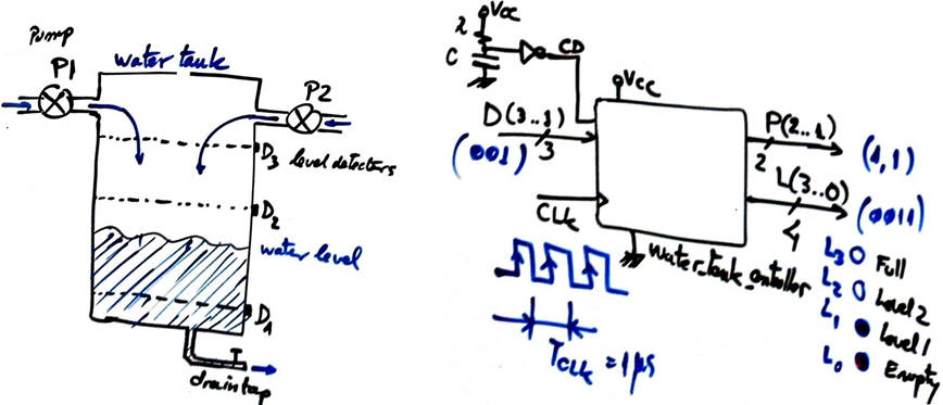
a) Represent the Water_tank_controller symbol and details.
 |
|
Fig. 2. Tank sketch and symbol. |
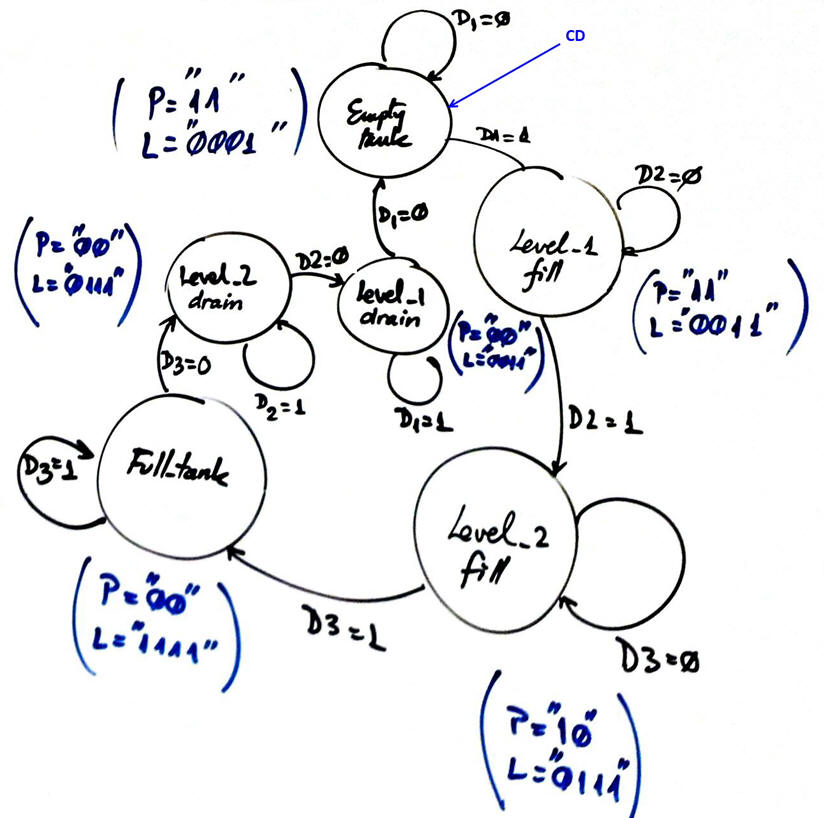
b) Draw the state diagram.
 |
|
Fig. 3. State diagram. |
c) Adapt the FSM architecture to this problem, naming and connecting all signals and inputs and outputs.
e) Sketch a timing diagram showing the main operations.
f) Draw the state register if coding the machine in Gray. How many D_FF of memory are used in this problem?
g) Write the CC2 truth table to obtain the outputs of the circuit and its flowchart.
h) Design the CC1 truth table to obtain the next state to go and its flowchart.
i) Write the VHDL file and start an EDA project to synthesise the circuit and obtain results. Inspect the RTL and verify that it looks like your schematic. Check the number of D_FF, print and comment the schematics. CLK oscillator is 1 MHz.
j) Write a VHDL test bench and run the EDA simulation tool to verify your design. Measure the maximum CLK frequency that can be applied to your design considering a target chip from Intel (Cyclone IV EP4CE115F29C7).
Optional. Other additional features:
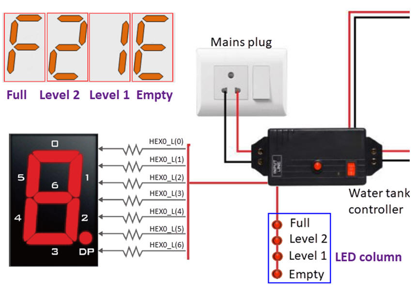
k) The user wanted to add an extra circuit to translate the LED column code into a 7-segment display. Thus, an additional combinational circuit CC3 is required to meet this new specification. Let us solve the problem using the ROM method for implementing logic functions. The wiring in Fig. 4 shows the naming conventions for the vector HEX0(6..0) common anode in the DE2-115 board user guide page 36. Discuss the size [2^m x n] of the ROM.
 |
|
Fig. 4. Enhancement with a 7-segment display. |
| Home Term 23/24-Q2 Contact Products Electronic devices and companies Software Books Magazines Instruments DEE Library EETAC DEEL |

|
|
| Web activa des de 09/2001, @ F. J. Robert, J. Jordana. Web editat amb Microsoft Expression Web 4. El contingut és un complement als materials d'estudi del curs Circuits i Sistemes Digitals disponibles al campus digital Atenea. Llicència:Reconeixement 4.0 Internacional de Creative Commons |