|
CSD_PICstick development board |
||
We can implement prototypes for simple circuits based on microcontrollers using standard commercial boards such as PICDEM2 or EXPLORER8. However, it is interesting and educational to design a custom training board for solving our introductory lab exercises.
| 1. Specifications | Planning | Developing | Testing | Report |
Let us conceive a simple training board containing these features:
- 40 pin and 28 pin sockets.
- Reset push-button.
- Primary and secondary XTAL oscillators.
- ICSP PIC chip program and debug using a commercial PICkit5, ICD5 or MPLAB SNAP device.
- Unregulated DC input VIN from 7 V to 15V.
- Selectable PIC voltage from VCC = +5V or +3.3V.
- 8 LED to represent binary codes (or a 10-LED bar).
- Active-low push-button at INT0.
- Switch at RA5.
- Analogue input at RA0.
- 20x2 header connector with all microcontroller pinning.
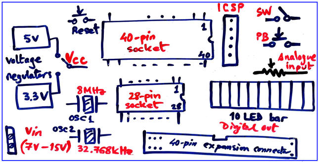 |
| Fig. 1. CSD_PICstick idea. Jumpers will be used to connect or disconnect some circuits. The 40-pin expansion connector allows the insertion of any daughter board. |
| Specifications | 2. Planning | Developing | Testing | Report |
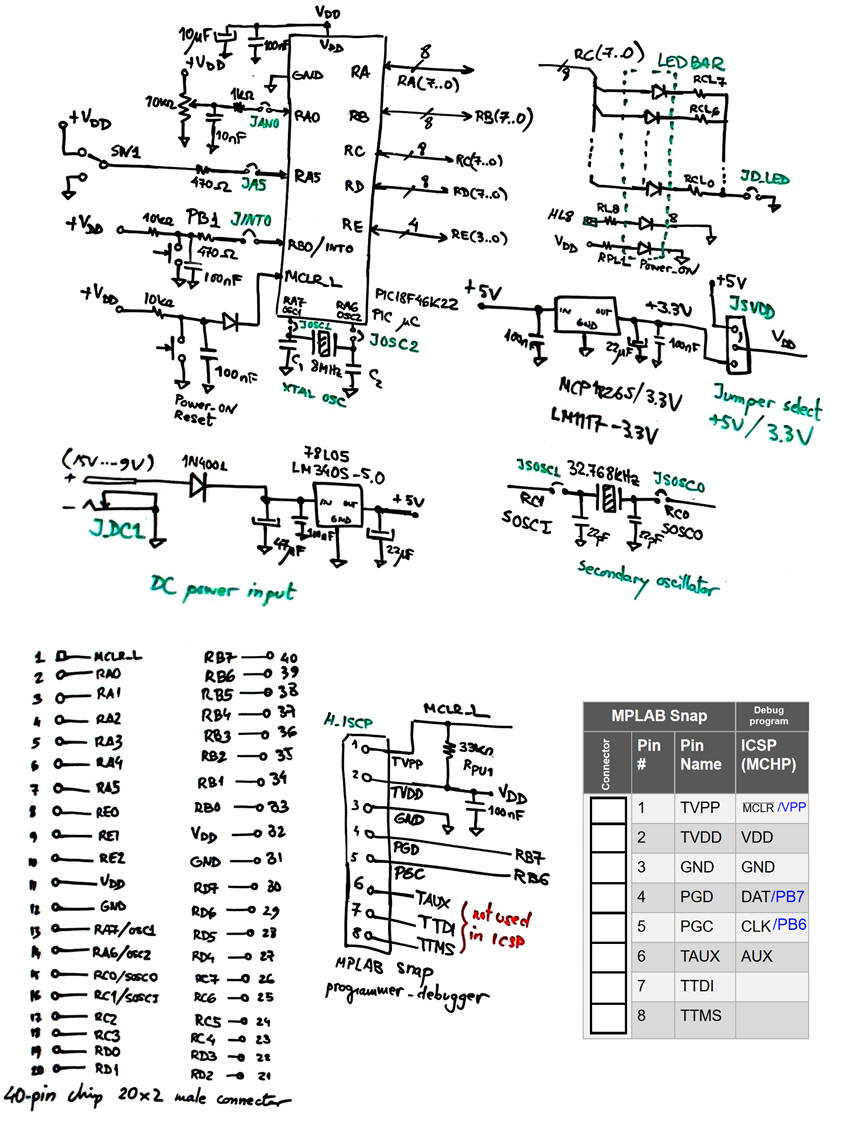 |
| Fig. 2. Ideas on the schematic. We will use 40-pin and also 28-pin mC sockets. |
| Specifications | Planning | 3. Developing | Testing | Report |
Proteus simulation
Before designing the PCB, we can try that the basic idea works correcty solving a given example in Proteus. For instance, let us solve the same Counter_BCD_1digit as a FSM using plan X proposed in LAB10 targeting a PIC18F46K22. This is the hardware circuit CSD_PICstick.pdsprj, and this the software C source program: CSD_PICstick.c. Basically only the configuration bits are adjusted to the new microcontroller.
PCB design
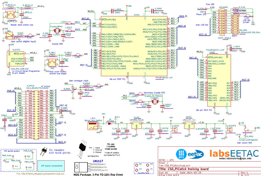 |
| Fig. 3. The PCB schematic contains many more resourcs, like headers, test points, etc. |
The full KiCad project PCB_CSD_PICstick_v1.zip.
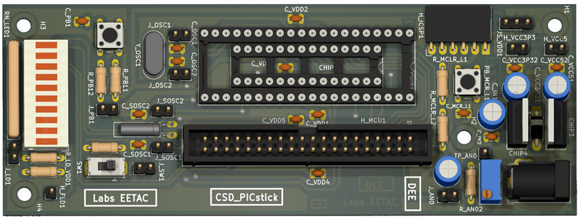 |
| Fig. 3. The 3D view of the finished board. |
| Specifications | Planning | Developing | 4. Testing | Report |
The board soldered and ready for testing an example project.
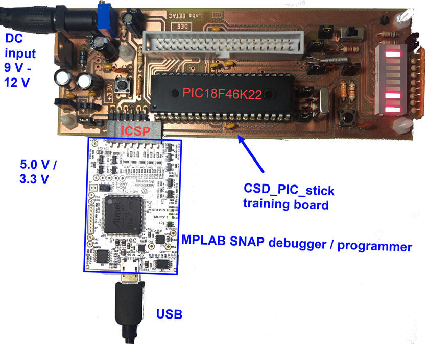 |
| Fig. 3. Prototype ready for running an application. |
| Specifications | Planning | Developing | Testing | 5. Report |
Project report: sheets of paper, scanned and annotated figures, file listings, notes or any other resources. In CSD follow this rubric of indications for writing reports.


