|
|
Bachelor's Degree in Telecommunications Systems and in Network Engineering |
|
|
|
||
|
|
6-bit binary radix-2 to BCD. Plan A: equations single-file VHDL (flat) |
|
|
|
||
Type 74185 standard commercial chip
1. Specifications
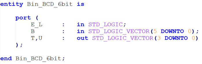
Design a 6-bit binary radix-2 to BCD converter as explained in Fig. 1, adapting to VHDL the circuit from the DM74185 datasheet using plan A structural approach. This is finding the circuit algebraic equations and writing them in VHDL.
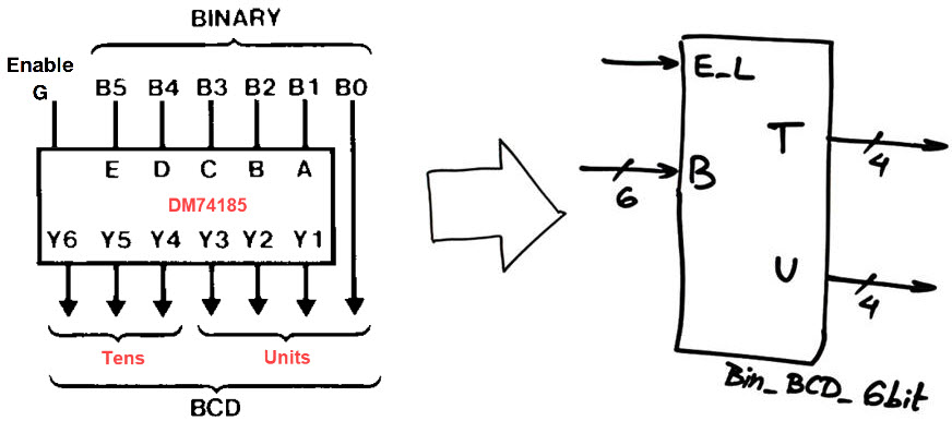 |
| Fig. 1. Bin_BCD_6bit symbol adapted from the chip DM74185. When the chip is desabled, we will implement the code 'dd'. Our symbol integrates the least significant bit (B0) is integrated in the chip. |
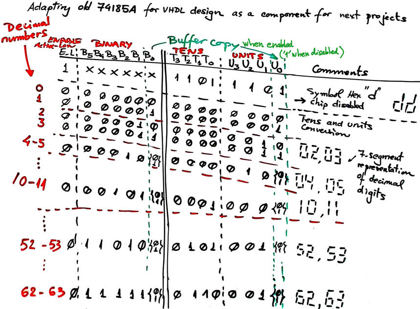
The circuit can be implemented adapting the datasheet truth table to our naming conventions as shown in Fig. 2.
 |
|
Fig. 2. Bin_BCD_6bit component truth table. This chip is capable of converting any 6-bit radix-2 number from 0 to 63 into BCD separating the units and tens digits. |
An example sketch of timing diagram to demonstrate how the circuit works for several input stimulus is presented in Fig. 3.
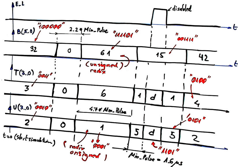 |
| Fig. 3. Example timing diagram. |
This is the article from Wikipedia: the double dabble algorithm is used to convert radix-2 numbers into BCD.
2. Planning
Plan A design flow. The idea is to translate the truth table in Fig. 2 into VHDL using equations.
Synthesis. Copy the table in Minilog format. Run Minilog.exe to obtain SoP or PoS.
Translate the equations to VHDL finding a similar file to adapt.
Choose a target chip and start a Quartus Prime project. Project and file locations:
C:\CSD\P2\Bin_BCD_6bitA/(files)
Inspect, print and discuss the RTL and technology views. How many chip resources are used in this design?
Verification. Start a testbench template.
Add to the template the Fig. 3 timing diagram as a stimulus process including also the Min_Pulse time constant.
Setup the wave diagam and run simulations.
3. Development
Write minimised (SoP or PoS) equations using Minilog.exe. For instance: truth table Bin_BCD_6bit.tbl and solution Bin_BCD_6bit_corrected_SoP.txt (or similarly, Bin_BCD_6bit_corrected_PoS.txt that is another circuit).
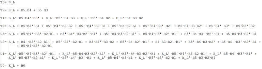 |
| Fig. 4. List of minimised equations in SoP format. |
Find a similar VHDL description for a plan A circuit, copy and adapt. This is the translation into VHDL: Bin_BCD_6bit.vhd
Fig. 5 shows the description of the entity accordingly to the CSD input and output naming in Fig. 1.
 |
| Fig. 5. Entity definition is the same whatever the plan. |
Start an EDA synthesis project named Bin_BCD_6bit_prj for a given target chip, for example Intel CPLD EPM2210F324C3 and examine results.
Fig. 6. RTL schematic of the Bin_BCD_6bit using structural description in SoP. |
The real technology view schematic, the synthesised circuit in the FPGA, shows the number of chip resources used in the design.
|
Fig. 7. Technology view of Bin_BCD_6bit targeting Intel CPLD: EPM2210F324C3. |
We can add to the report the representation from the Chip Planner tool, as shwon in Fig. 7.
|
Fig. 8. The Chip Planner tool in Quartus Prime can be used to locate exactly where your circuit is synthesised in the FPGA lattice of logic cells. |
4. Testing
In Fig. 9 is represented the testbench schematic to stimulate the unit under test (UUT) with input vectors. In a step #1 generate the skeleton of the testbench file, in a step #2 add stimulus translating to VHDL input activity from the time diagram in Fig. 2. This is an example of a simple test bench Bin_BCD_6bit_tb.vhd from which you can copy the constant Min_Pulse and the stimulus process.
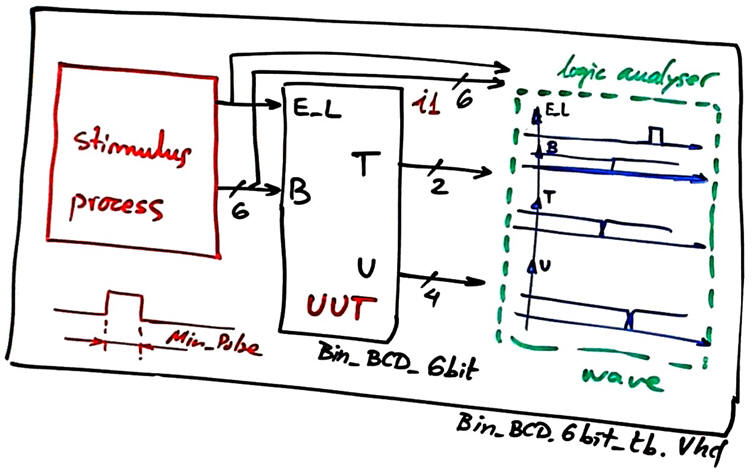 |
| Fig. 9. Testbench fixture to verify that our circuit works as expected. |
Start the VHDL simulator project, Bin_BCD_6bit_functional_sim, and run the test. Verify applying sufficient test vector that the device works as expected (verify how the information of each channel is selected). Print timing diagram screen and add comments on the signals to show how the device works.
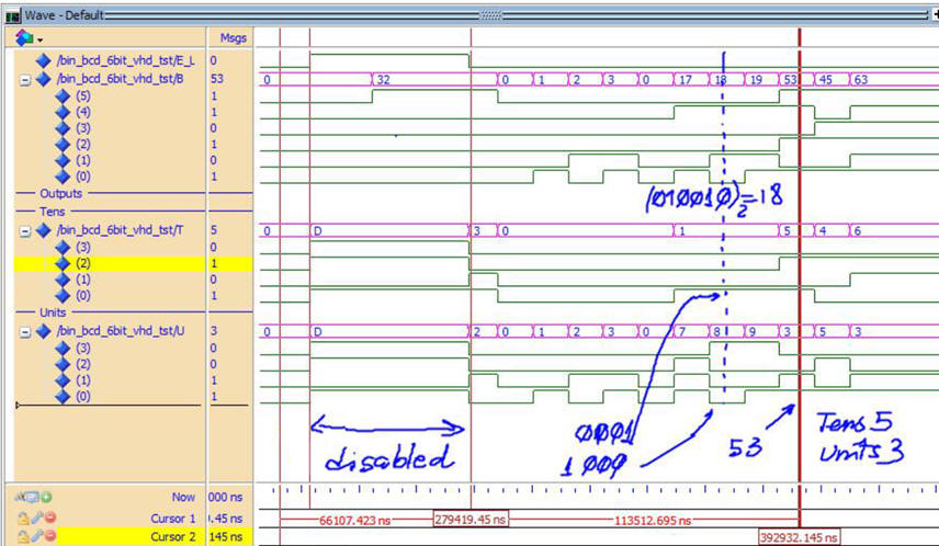 |
| Fig. 10. Ideal functional simulation waveform results from the logic analyser. |
5. Report
6. Prototyping
| Home Term 24/25-Q1 Contact Products Electronic devices and companies Software Books Magazines Instruments DEE Library EETAC DEEL |

|
|
| Web activa des de 09/2001, @ F. J. Robert, J. Jordana. Web editat amb Microsoft Expression Web 4. El contingut és un complement als materials d'estudi del curs Circuits i Sistemes Digitals disponibles al campus digital Atenea. Llicència:Reconeixement 4.0 Internacional de Creative Commons |