|
L8.1: Dedicated processors [P8] Advanced digital System architecture: Datapath + Control unit + CLK generator |
[19/11] |
2.8. Dedicated processors or subsystems
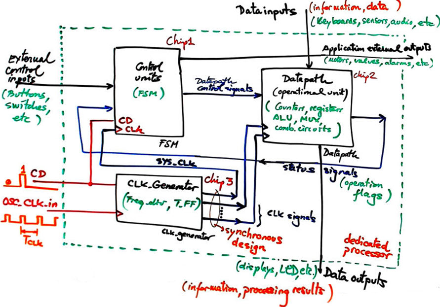
Note: In our introductory course, the concepts dedicated processor, subsystem, advanced or complex digital system, will refer to the same unified architecture represented in the figure below:
2.8.1. Unified architecture of an advanced digital system
We can study the P8 highlighted project Timer_MMSS as an example of dedicated processor.
As another example of advanced digital circuit, run the HH:MM:SS real-time clock available in Proteus.
2.8.2. Datapath (or operational unit)
Datapath may contain components for inputting, registering, operating and outputting information such as: registers, memories, code converters, parity generators and checkers, multiplexers, decodes, encoders, counters, ALU (add, subtract, multiply, shift, count, OR, AND, etc.) and simple logic. Indeed, circuits from P1, P2, P3, P4, P5 and P7.
And, as a result of performing operations, the datapath will generate status signals for the control unit such as zero, terminal count, overflow, negative, etc.
2.8.3. Control unit (FSM).
A single file plan C1 synchronous standard FSM like all the examples discussed in P6.
Such unification implies that we can apply all our course contentfor solving our projects.
Exercise: Design the block diagram of a 10-bit serial adder. The datapath contains only an Adder_2bit as the component to perform operations. Complete the datapath and explain the required state diagram in the control unit. Analyse this similar tutorial Adder_4bit serial adder to get the notions to infer the block diagram of this dedicated processor.


