|
|
Bachelor's Degree in Telecommunications Systems and in Network Engineering |
|
P8: Dedicated processors (datapath, control unit, CLK generator) |
| Resources in lectures and labs: | L8.1, L8.2. | Project | objectives |
|
|
Highlighted project: MM:SS programmable timer, CLK generator
1. Specifications
The idea is to invent a timer circuit (Timer_MMSS) for counting down a programmable timing period up to one hour.
|
|
| Fig 1. Front panel with main details of the Timer_MMSS application. |
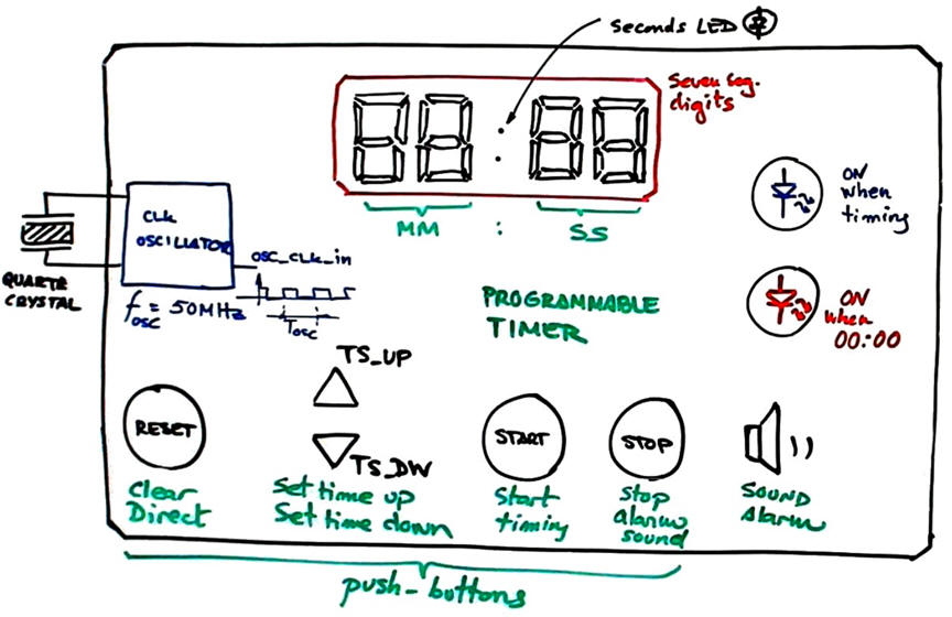
Circuit's symbol is shown in Fig. 2. User can program the timing period clicking time-set up and down (TS_up, TS_down) pushbuttons.
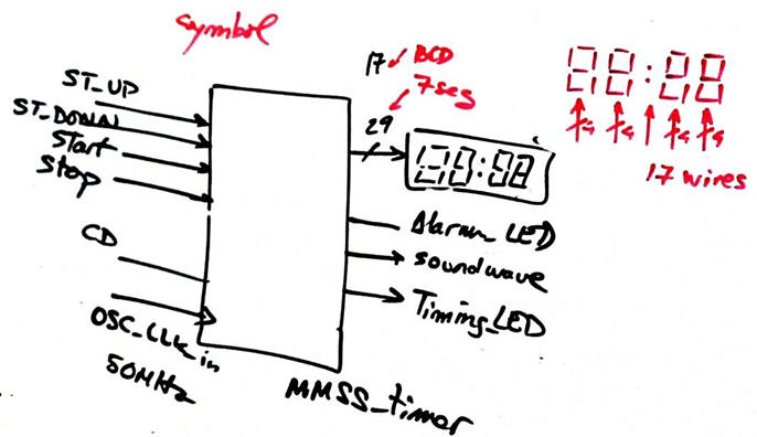 |
Fig 2. Symbol and signal naming. |
The complete set of specifications and an example of timing diagram is represented in Fig. 3.
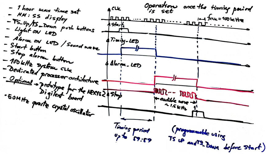 |
| Fig 3. Specifications and example timing diagram. |
Our programmable timer will include the component CLK_Generator to derive all the system synchronous CLK signals from the same external 50 MHz quartz crystal oscillator.
This is a complex project where we recommend practising teamwork (1), project and time management (2) and English (4).
Organise the general architecture of the Timer_MMSS in Fig. 2 as a dedicated processor.
Target boards and programmable chips: Xilinx Digilent Nexys2, Intel Terasic DE0, DE10-Lite.
|
|
Other design tutorials and assignments.
2. Planning
Fig. 4 represents the general framework of an advanced digital system or dedicated processor. Many applications and subsystems can be created using this powerful plan C2: data transmitters and receivers, A/D and D/A converters, digital filters, timers, etc. Many microcontroller peripherals are planned in this way.
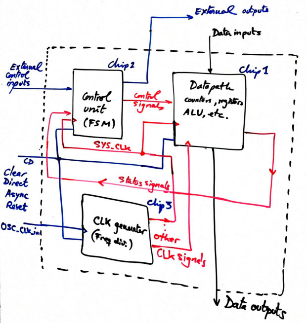 |
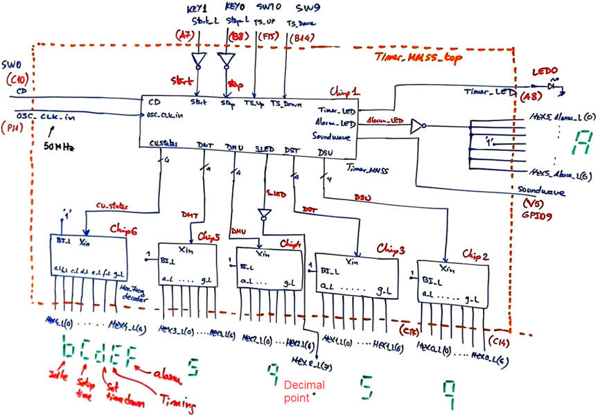
Fig. 4. General architecture for a dedicated processor. Chip 1: Datapath is in charge of performing operations with input data or information. Chip 2: Control unit, a FSM, is in charge of sequencing the algorithm or the flowchart. Chip 3: CLK_Generator circuit is required to implement synchronous CLK signals derived from the same external high frequency quartz crystal oscillator. |
The dedicated processor architecture adjusted to this project is represented in Fig. 5.
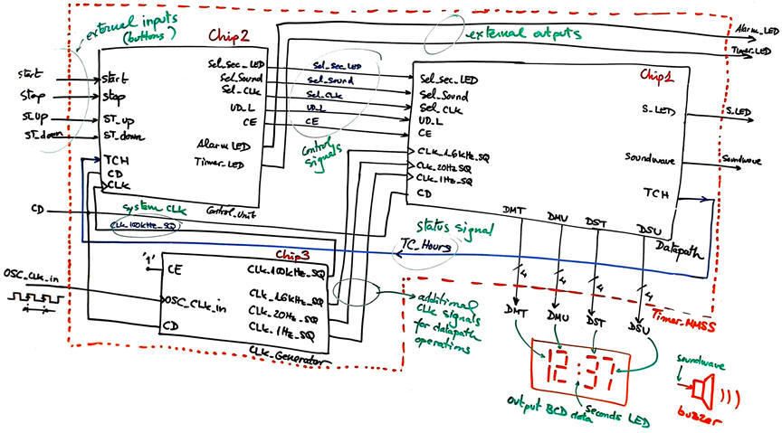 |
| Fig 5. Dedicated processor main blocks. |
Datapath. The main component in the datapath is the Counter_MMSS (modulo 3600) in BCD with outputs organised in minutes and seconds to drive 7-segment displays. The internal design of the Counter_MMSS is discussed below in Annex 1.
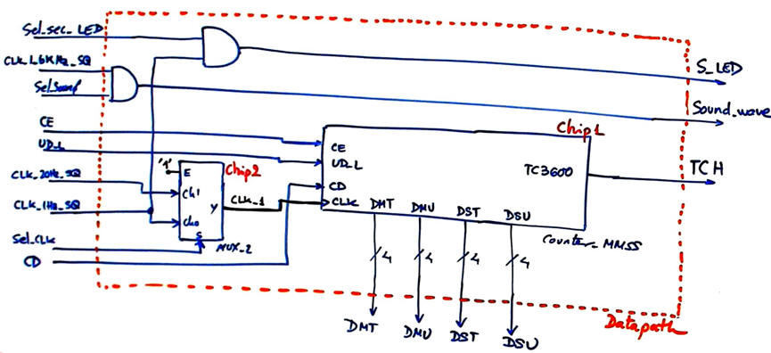 |
| Fig 6. Datapath internal architecture. |
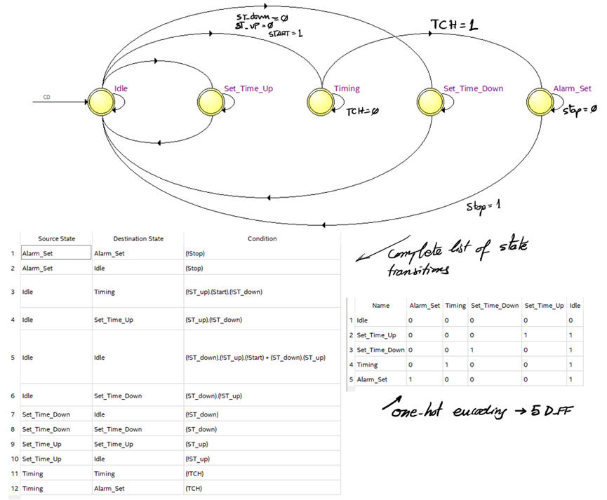
Control unit. The idea and state diagram is sketched in Fig. 7. Its aim is to interface input buttons, generate internal control signals for managing the datapath, and generate external outputs. This block is designed following our standard FSM procedure as any other P6 application.
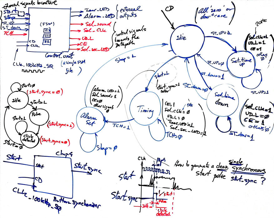 |
| Fig 7. Control unit symbol, signals and state diagram ideas to organise the FSM. |
Chip 3 CLK_generator will supply all synchronous CLK signals for the dedicated processor. It is our standard hierarchical circuit based on plan C2. Its internal design is discussed below in Annex 2.
This is the project location:
C:\CSD\P8\Timer_MMSS\(files)
3. Developing
At this stage, the process to follow is a bottom-up sequence: (1) design each block in the architecture using components from digsys, (2) complete the top entity.
We can choose the target chip MAX10 10M50DAF484C7 so that at step 6 we can prototype the circuit in the DE10-Lite board.
Step 1.- Plan, synthesise and test the component Chip1 Counter_MMSS in Fig. 6. Its full project is reported below in Annex 1.
Step 2.- Plan, synthesise and test the component Chip3 CLK_generator in Fig. 5. Its full project is described in Annex 2.
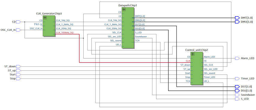
Step 3.- Synthesise and test the complete dedicated processor Timer_MMSS in Fig. 5. Testing the components Control_unit or Datapath separately is too complicated, and at this level is better to tackle all the project. Example files: Timer_MMSS.vhd, MUX_2.vhd, Datapath.vhd, Control_unit.vhd.
  |
|
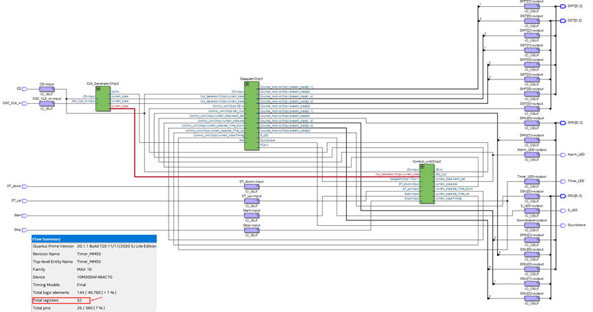
Fig 8. RTL for the full project .The Control_Unit state diagram is coded in one-hot. |
Project summary indicates that up to 52 D_FF are used.
 |
|
Fig 9. Technology view for the full project Timer_MMSS. |
While examining EDA results, project summary, RTL and technology schematics, be aware of the number of registers (D_FF) used in the target chip and justify the value. Does it match your initial estimation?
4. Testing (functional)
Complete the template test bench file and run the EDA tool.
 |
|
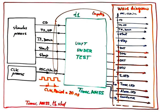
Fig 10. Initial testbench fixture. To follow how the machine is running the state diagram, descent the hierarchy and add internal signals to the wave diagram, such SYS_CLK and current_state. |
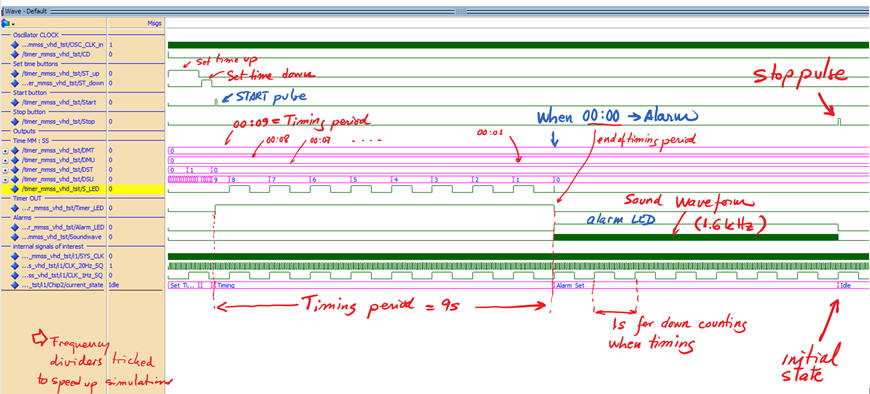
Print some timing diagrams and analyse that the circuit works fine in all situations. Fig. 11 is an example.
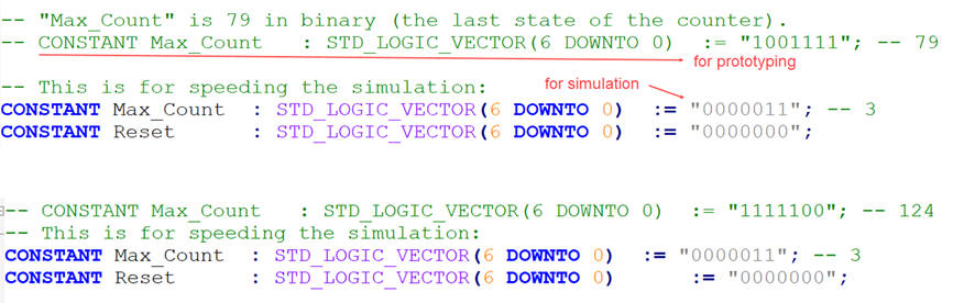
Frequency dividers has to be tricked to speed up simulations, for instance, instead of dividing by 125, let it divide by 3. Remember that Start and Stop pulses must be longer that SYS_CLK period. This is an example Timer_MMSS_tb.vhd and a wave setup wave.do.
  |
|
Fig 11. Simulation results. |
In this application, preparing testbench stimuli and running simulations is not that simple, and it is clear that for such complex real-time circuits board prototyping and laboratory experimentation is a better option.
5. Testing (gate-level, timing analyser)
Optional. Gate-level and timing analyser can be used for proposing new questions and further research. For example:
- What is the time precision of such programmable timer?
- How the value of the SYS_CLK frequency can affect timer performance? In this application we have chosen 100 kHz. What may be the difference if we select 10 MHz?
- How to invent a programmable timer in the range of tens of nanoseconds?
DE10-Lite board (Intel FPGA, Terasic)
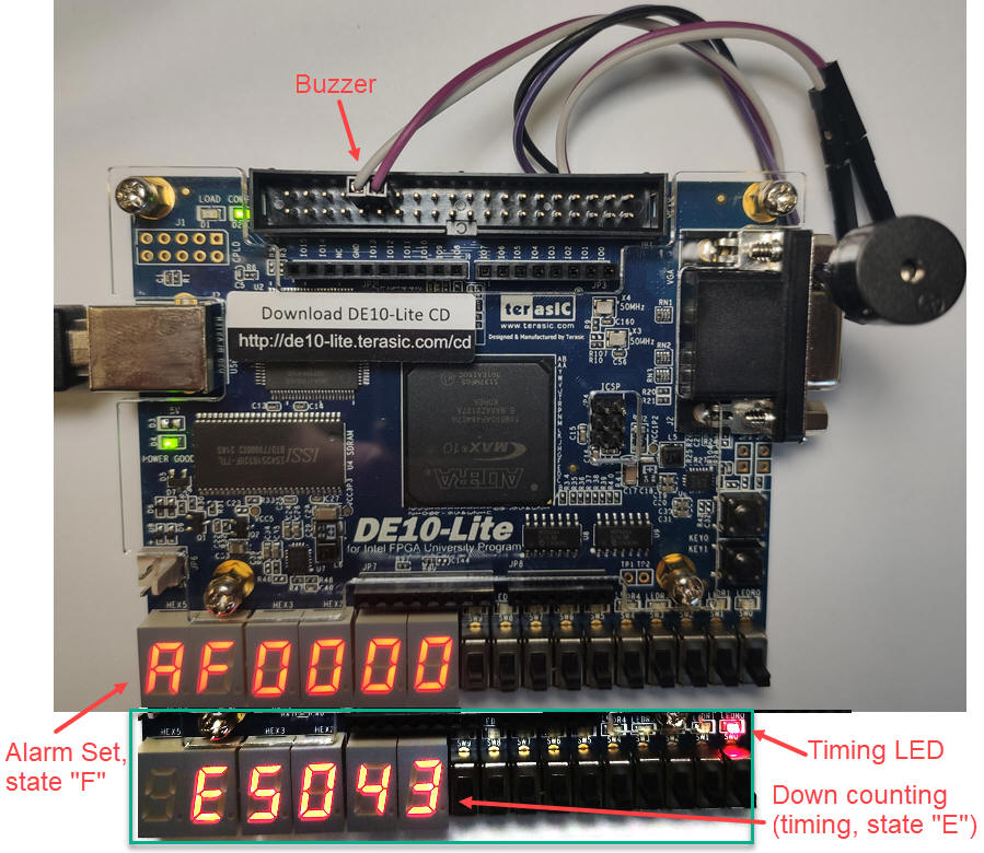
Prototyping the Timer_MMSS in a DE10-lite board. Organise a Timer_MMSS_top circuit to condition buttons, LED and displays.
 |
|
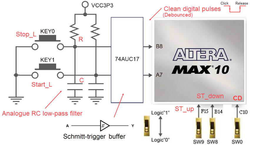
Fig 12. Switches and keys used as inputs. Switches generates both digital values, Pushbuttons are active-low, |
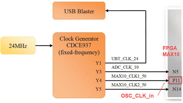 |
Fig 13. 50 MHz OSC_CLK_in signal from the board's CLK subsystem, a CLK generator chip itself. |
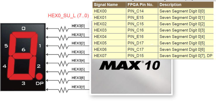  |
| Fig 14. LEDs are active-high. 7-segment displays are active low. Each segment is connected to an FPGA pin. |
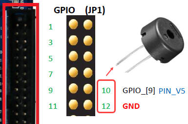 |
Fig 15. Piezo buzzers are used for making beeps and alerts. We can them using square waves from 3 V to 30 V. Connect one pin to GND (either one) and the other pin to a square wave out from your digital circuit. For instance, the expansion connector GPIO9 (pin V5). We will apply the squared 1.6 KHz frequency signal named Soundwave. |
We can use one of the free displays for representing the signal Alarm_LED as character "A". And we add a new output at the Control unit to monitor the internal current state of the machine in another free digit.
 |
|
Fig 16. Complete schematic Timer_MMSS_top.vhd |
This is the Timer_MMSS_top_prj_pin.csv pin assignment file list that you can import to your Quartus Prime project. This is the final Timer_MMSS_top_prj_pin.sof to program the chip. This is the complete file list Timer_MMSS_top.zip included in this prototype experiment.
 |
|
Fig 17. Prototype running. |
Nexys 2 (Xilinx FPGA, Digilent)
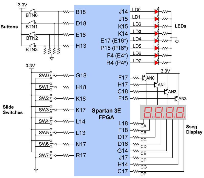
Additional circuit are required for adapting the design to 7-segment displays available on some training boards. For instance, if we consider the Nexys2 board from Digilent, as shown in Fig. 1, a multiplexed display system (MDS) has to be implemented because all the four digits available share the same A, B, C, D, E, F, G segments outputs.
 |
|
Fig 1. Buttons, switches, LED and 7-segment displays hardware connections on board Nexys2. |
The proposed MDS is represented in Fig. 2. We can drive the MDS from the 1.6 KHz squared signal available in the project.
 |
|
Fig 2. Multiplexed display system (MDS) to drive all the four 7-segments displays with output data from Timer_MMSS. |
This is the complete project Timer_MMSS list of files for Nexys 2. In the laboratory we can experiment measuring circuit performance.
7. Report
Follow this rubric for writing reports.
Annex 1: Counter_MMSS: plan, development and test.
Specifications
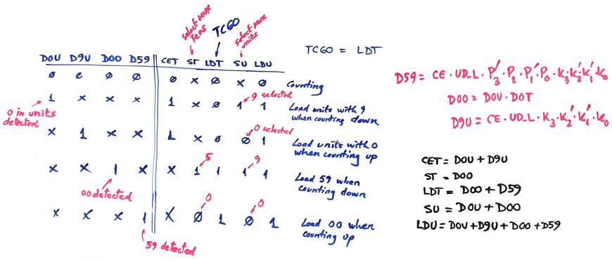
Design the Counter_MMSS circuit used as Chip1 in the dedicated processor datapath (Fig. 6 above), the symbol of which is drawn in Fig. 1. It is a 4-digit BCD counter module 3600 divided in two chained SS (modulo 60) and MM (modulo 60) synchronous counters.
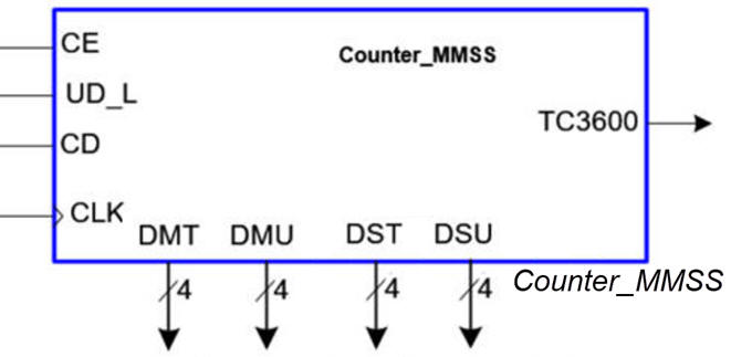 |
| Fig 1. Symbol. |
Plan
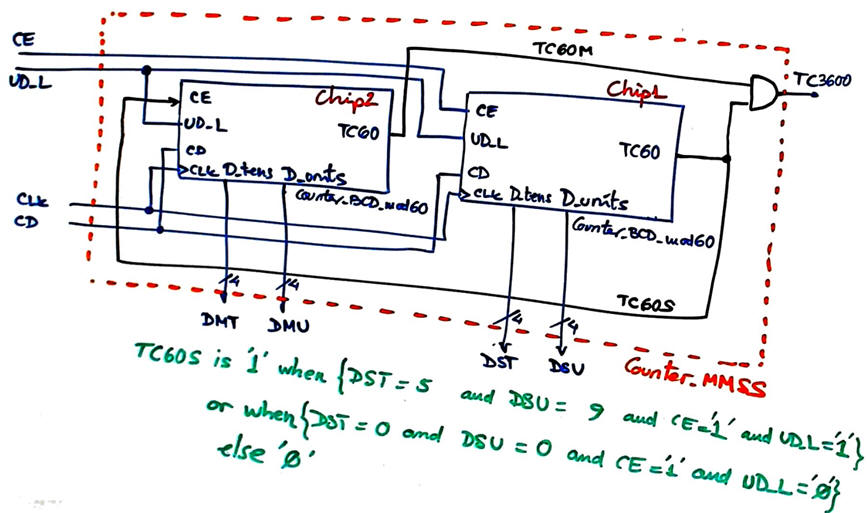
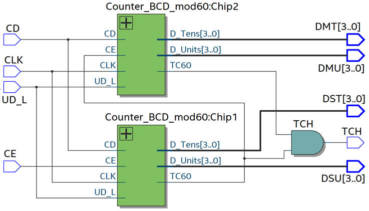
As represented in Fig. 2, Counter_MMSS can be invented expanding Counter_BCD_mod60 devices.
 |
|
Fig 2. Inventing the Counter_MMSS (visio) requires chaining Counter_BCD_mod60 blocks for counting seconds and minutes. |
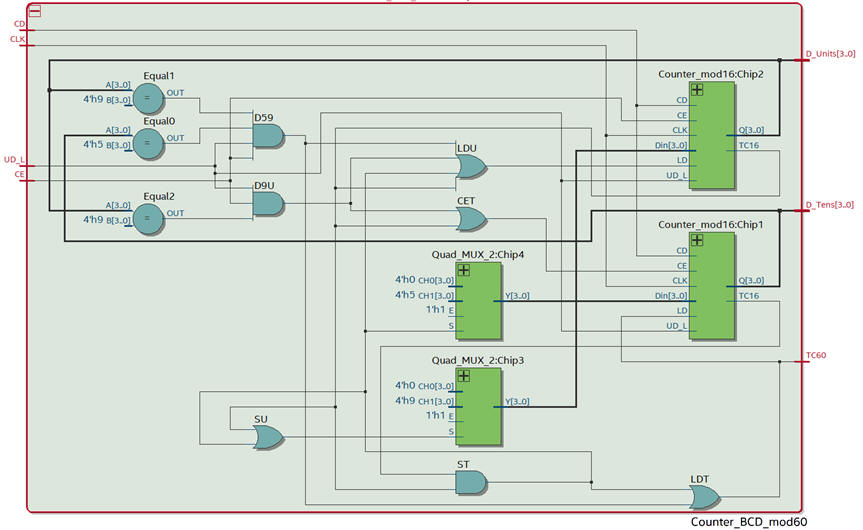
Inventing the Counter_BCD_mod60 requires chaining Counter_mod16 components using truncation techniques in the way discussed at P7.
 |
|
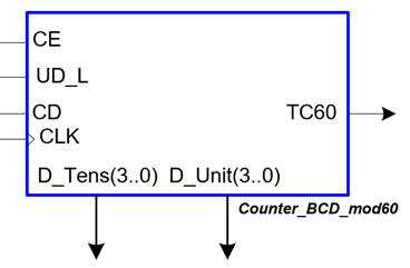
| Fig 3. Proposed internal architecture for Counter_BCD_mod60. |
Project location:
C:\CSD\P8\Timer_MMSS\Counter_MMSS\(files)
Development
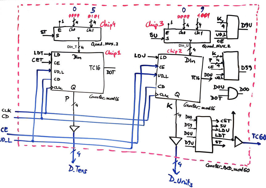
Example file translation of schematics above in Fig. 2 and Fig. 3: Counter_MMSS.vhd, Counter_BCD_mod60.vhd, Quad_MUX_2.vhd, and copy the Counter_mod16.vhd from its plan Y tutorial Counter_mod16.
  |
|
Fig 3. Top Counter_MMSS RTL circuit and its component Counter_BCD_mod60. built chaining basic Counter_mod16. |
Total number of registers D_FF is 16. Total logic elements is 79.
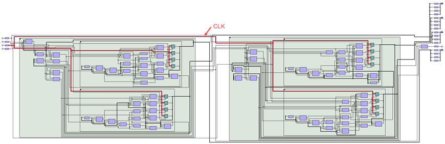 |
Fig 4. Technology view emphasising how the CLK signal is distributed to all 16 D_FF. (pdf) |
Test
We need to drive CLK, CD, CE and UD_L in the usual way.
Generate from Quartus Prime the VHDL testbench fixture skeleton. Rename it and move it to the project folder.
Copy from this example file Counter_MMSS_tb.vhd only the stimulus activity described in the two processes and also the constant CLK_Period.
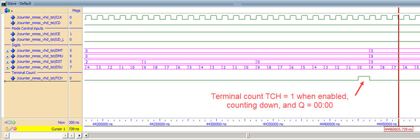
Start and run a functional simulation project using ModelSim to verify that the device operates correctly. Let us try one mode of operation at a time. For instance, Fig. 5 shows how the circuit is counting down. It need a time of 3600·CLK_Period to complete all counting range.
 |
|
Fig 5. Simulation results. |
Annex 2: CLK_Generator project: plan, development and test
Specifications
In this application are required up to four square CLK signals at 100 kHz (system CLK), 1.6 kHz (sound wave), 20 Hz (time set up and down) and 1 Hz (timing). We will consider a 50 MHz input OSC_CLK_in.
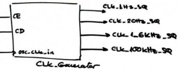 |
Fig. 1. Symbol of the CLK_generator required for our Timer_MMSS. |
Planning
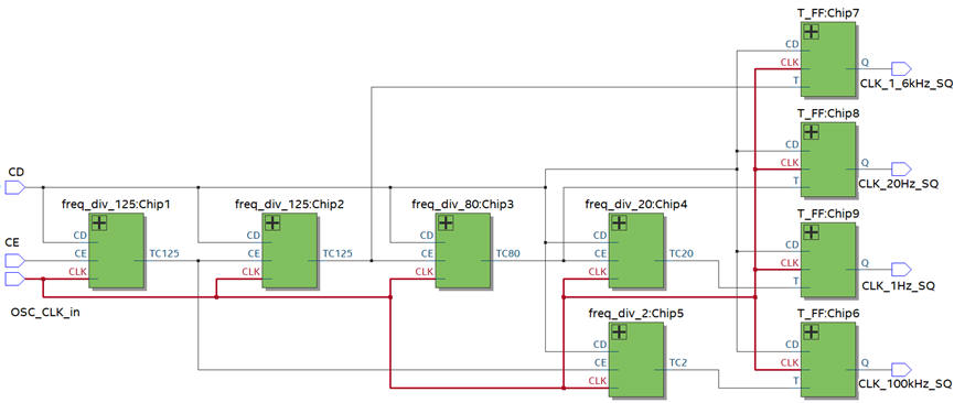
As discussed in L8.2, we will use the generalised schematic that works chaining frequency dividers (freq_div_Mod, plan Y) and T_FF for squaring the waveforms. The objective is to build this circuit below in order to generate all the necessary squared waveforms for the Timer_MMSS.
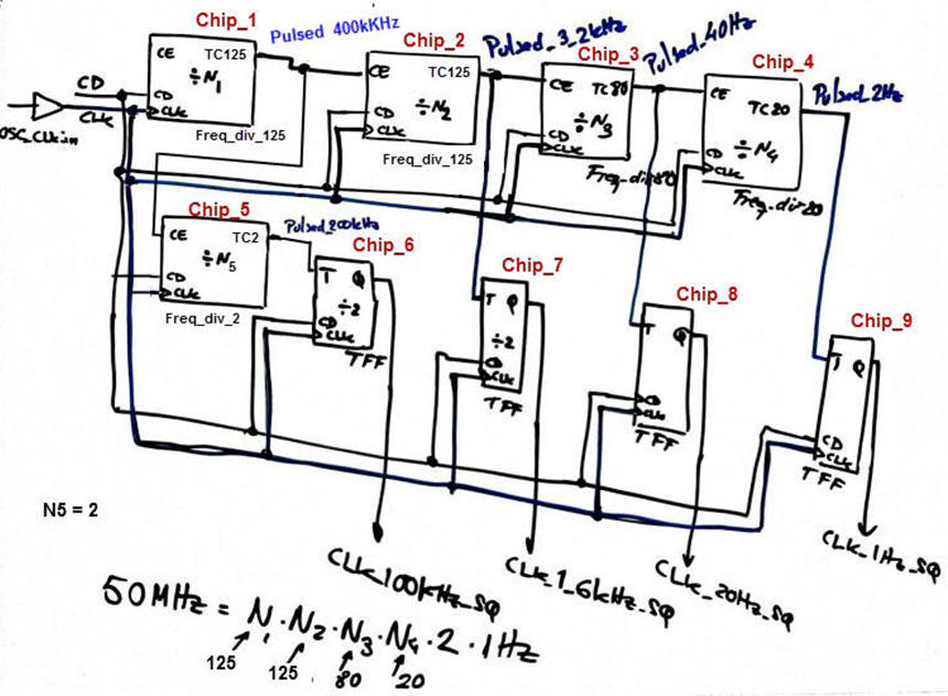 |
| Fig. 2. CLK_Generator architecture based on frequency dividers and T_FF memory cells. |
Fig. 3 shows a picture of the 50 MHz quartz crystal populating the Altera DE0.
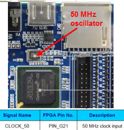 |
Fig. 3. Intel DE0 board 50 MHz oscillator from which we will derive the synchronous squared CLK signals of: 100 kHz, 1.6 kHz, 20 Hz, and 1 Hz required in this project. |
Another board like DE10-Lite has two identical 50 MHz CLK signals available for the FPGA at pins P11 and N14 from its own CLK generator: a specialised chip CDCE937.
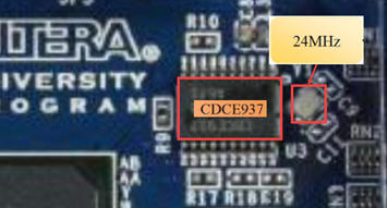 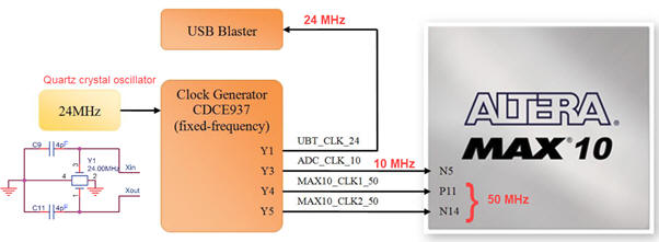 |
Fig. 4. Intel DE10-Lite board CLK circuit derived from a 24.00 MHz quartz crystal. |
Project location:
C:\CSD\P8\Timer_MMSS\CLK_Generator\(files)
Development
Example files for translating to VHDL the schematic in Fig. 2: CLK_Generator.vhd, freq_div_125.vhd, freq_div_2.vhd, freq_div_20.vhd, freq_div_80.vhd, and get the T_FF.vhd file from its tutorial T_FF.
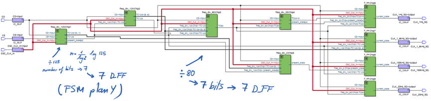
Picking up the FPGA MAX10 10M50DAF484C7G available in DE10-Lite board, we synthesise the RTL circuit represented in Fig. 5.
 |
|
Fig 5. CLK_Generator RTL schematic. We can check that this application requires 31 D_FF. |
 |
|
Fig 5. Technology view of this synchronous design. |
Test
Generate an skeleton of the testbench for simulating the CLK_Generator circuit. This is a valid testbench file CLK_Generator_tb.vhd from which to copy stimulus and CLK processes. CLK_Period = 20 ns.
Hint: in case of simulating the CLK_Generator as a component, because it is about counting tens of millions of pulses, there is a way to speed up the simulation tricking the frequency dividers while keeping the number of registers used and everything else, as shown in Fig.6. The output waveforms will be of different frequencies, but they will be synchronous and identical as in the real CLK_Generator which has to be configured in the real hardware.
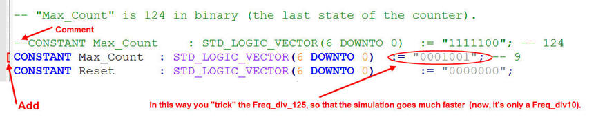 |
| Fig. 6. Modification in the VHDL code to speed up the simulations of the CLK_Generator component. |
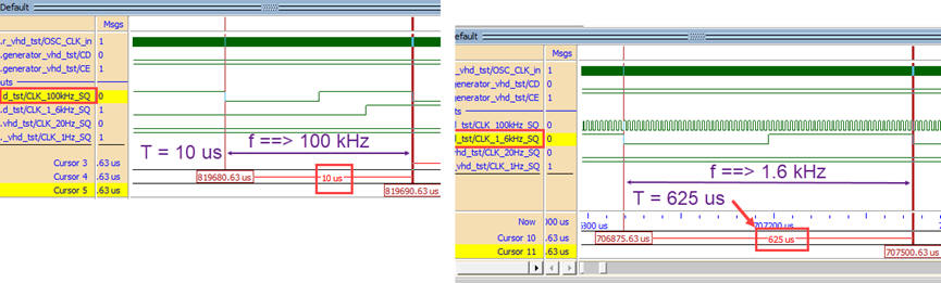
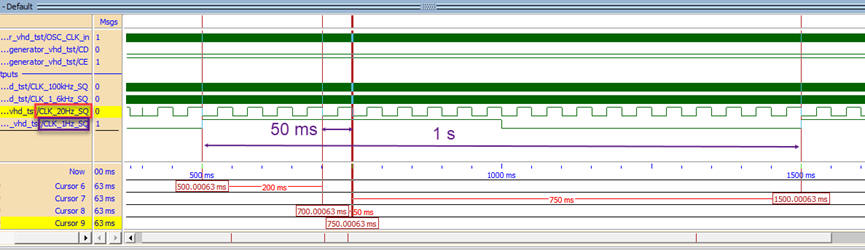
Zooming through the time scale and using cursors we can measure waveform periods and frequencies.
  |
|
Fig 7. Simulation results representing CLK waveforms pictured at different time scales. |
| Home Term 24/25-Q1 Contact Products Electronic devices and companies Software Books Magazines Instruments DEE Library EETAC DEEL |

|
|
| Web activa des de 09/2001, @ F. J. Robert, J. Jordana. Web editat amb Microsoft Expression Web 4. El contingut és un complement als materials d'estudi del curs Circuits i Sistemes Digitals disponibles al campus digital Atenea. Llicència:Reconeixement 4.0 Internacional de Creative Commons |