|
|
Bachelor's Degree in Telecommunications Systems and in Network Engineering |
|
P9: Introducing microcontrollers (μC). Digital I/O and programming |
| Resources in lectures and labs: | L9.1, Lab9, L9.2, L9.3, L9.4, | Project | objectives |
|
|
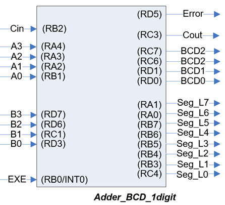
Highlighted project: 1-digit BCD adder (design phase #1)
1. Specifications
- The aim of this project is to solve a combinational circuit 1-digit BCD adder (Adder_BCD_1digit) using a microcontroller μC. This goal implies:
1) Getting in touch with a commercial μC from Microchip, for instance PIC18F4520, learning how to compile C language code using MPLABX+XC8 tools and simulate the project using Proteus. And also:
2) Study how C code is organised in CSD, configure digital inputs and outputs and connect program variables to pins using bitwise operations (OR, AND, etc.)
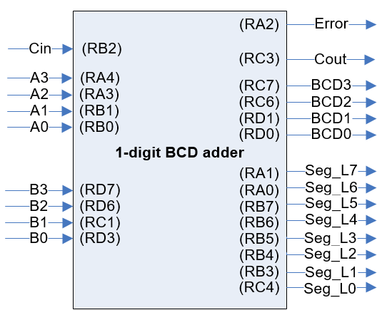 |
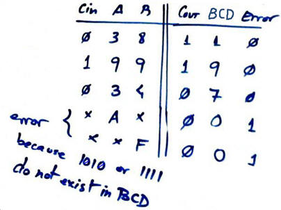
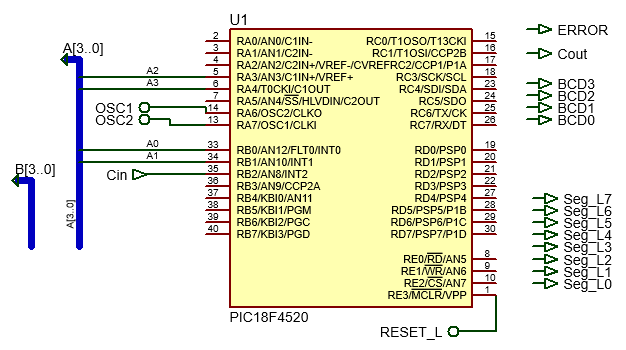
Fig 1. Symbol (Visio) of the 1-digit BCD adder indicating the port pins where to connect input and outputs. Solve the truth table of this device which is very similar to the classic chip MC14560 represented in Fig. 2. You may wonder why an error signal is required in this chip. |
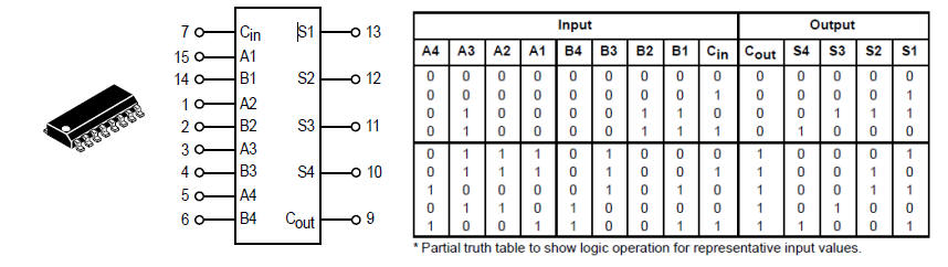   |
| Fig 2. Classic chip MC14560 that we try to recreate as a way to learn on digital inputs and outputs and code organisation in a microcontroller. This chip is not new for you because it could have been proposed in P3 as another arithmetic circuit, thus we will concentrate our efforts in the new μC technology to implement it. |
|
|
Other design tutorials and assignments.
2. Planning
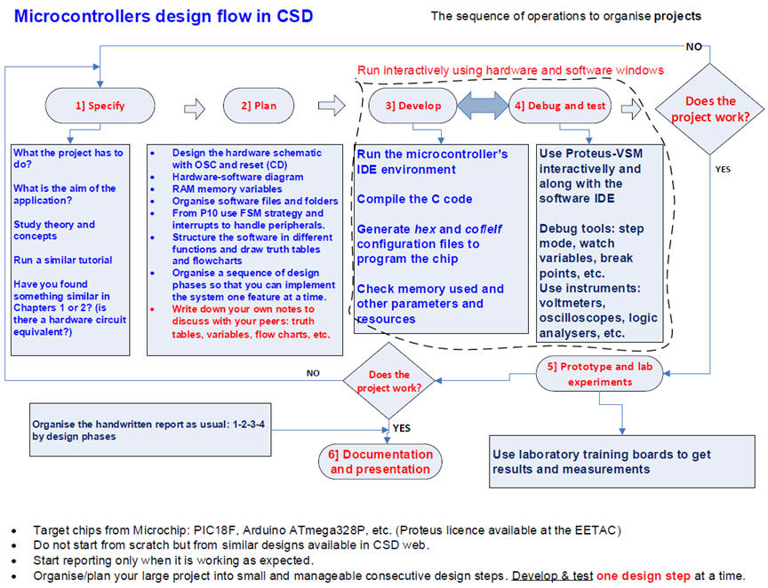
The design flow (Visio) is explained in Fig. 3 below.
 |
| Fig 3. Design flow using microcontroller technologies and development tools. |
A) Planning hardware
Draw your circuit in a sheet of paper and discuss where to connect: Reset (CD), crystal oscillator and digital I/O.
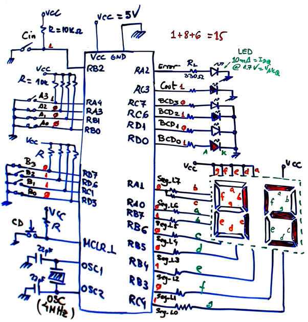 |
| Fig 4. Hardware schematic. |
B) Planning software
Our CSD style is reflected in the new conceptual tool for representing how to put into practice our design ideas: hardware-software diagram, as represented in Fig. 5. The key point is to define RAM variables (char, int, double int, etc.) that will allow the processing of the algorithms without regarding the way the PORT pins have been read or written. Thus, the kernel of the code (in this case truth_table() function) is hardware independent. Pay attention on hardware-dependent functions (input, output and system initialisation) and software (or platform independent) functions (the truth table) drawn using different colours.
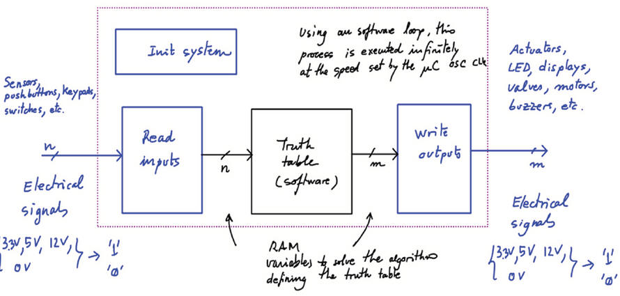 |
Fig 5. The new conceptual representation tool: hardware-software diagram. |
Organise the source code as in Fig. 6 using program flowcharts: Init_system(), read_inputs(), truth_table() (which is the algorithm or data processing) and write_outputs().
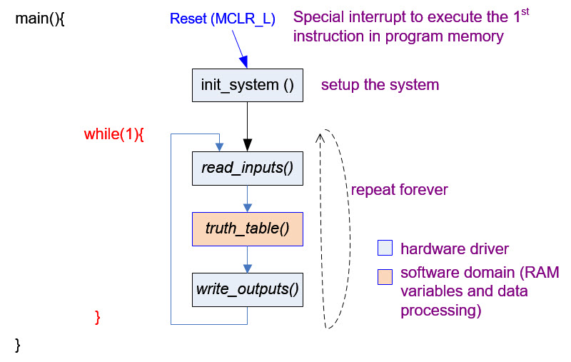 |
| Fig. 6. Proposed software organisation flowchart in CSD. |
RAM variables (Var_SEG_L is not yet represented, and this is not a problem, because you can add new features to your basic project later, once it works; this is the important idea of planning several design phases).
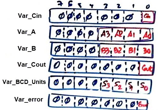 |
Fig. 7. Example of some convenient variables "Var" that will allow the processing of information in truth_table() independently of the microcontroller hardware. Program variables will be stored in RAM memory addresses and so, they are volatile. |
When we initialise the system, we configure microcontroller bi-directional port-pins to be unidirectional: only inputs or only outputs. Here, we will consider all unused port pins outputs as default. We do this configuration using the Tri-State Control Register (TRISx) bits. Saving a zero ('0') means output. Saving a one ('1') means that the pin will be an input. More information on pin configurations and tri-state technology.
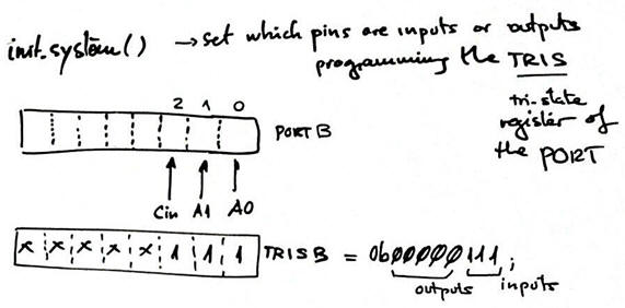 |
| Fig. 8. init_system() function details. Shadow register TRISx values, bits of interest. |
Read inputs. How to capture and transfer input voltages into RAM variables
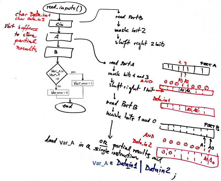 |
| Fig. 9. read_inputs() function: flowchart, operations, memory diagram, bits of interest, etc. |
Write outputs. How transfer RAM variables into port pin digital voltages.
 |
Fig. 10. write_outputs(). |
Behavioural plan B for translating a truth table into a flowchart and C language.
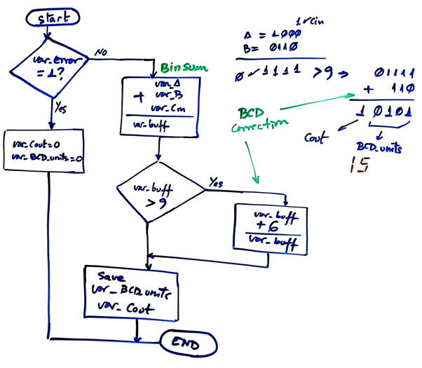 |
Fig. 11. truth_table() function flowchart. Use basically rhombus or diamond for decisions or yes/no questions and rectangles for actions or operations. |
Plan a sequence for building and debugging the application: the idea is "plan & develop & test" step by step introducing a few lines of code at a time. For instance:
1) Solve the code for reading only the Cin pin, compile, run and test the Var_Cin variable using the watch window.
2) Add the code for reading only the operant A, run, test and watch Var_A, etc.
NOTE: You may also consider several design phases. For instance:
Step #1. Solve the circuit using only switches, buttons and LED as represented in Fig. 5. And only when the system is working correctly,
Step #2. Add the extra RAM variables and modify the hardware and software to interface the 7-segment display.
Project locations and file names:
C:\CSD\P9\Adder_BCD_1digit\(files)
3. Developing and 4. Testing interactively
A) Developing hardware
Draw the schematic of the application in Proteus copying an example or tutorial which already contains the microcontroller that you have to use.
-
Target μC PIC18F4520: Adder_BCD_1digit.pdsprj
-
Target μC Atmega8535: Adder_BCD_1digit.pdsprj
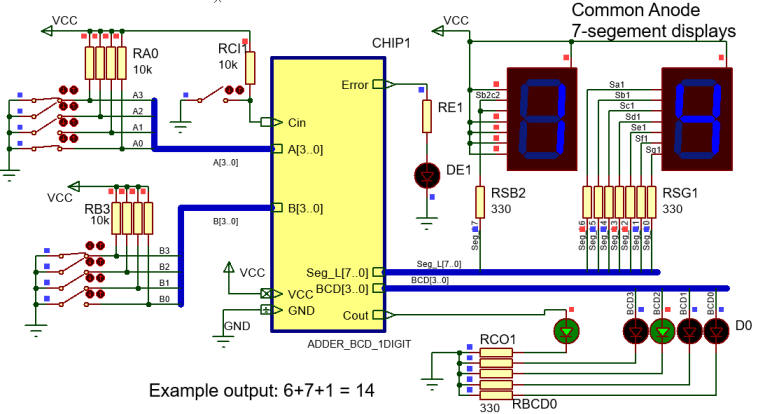  |
|
Fig. 12. The Adder_BCD_1digit symbol and electrical connections as captured in Proteus. Below you can see the internal architecture (child sheet) based on the PIC18F4520 where only some connections are completed. |
B) Developing software
Install MPLABX + XC8 software development environment
Run the microcontroller's IDE to develop and compile the C code copying and adapting an example code.
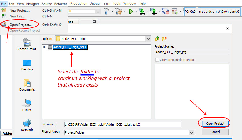
NOTE: If your project was created in a previous session and you like to continue working with it, simply click Open project and select the folder.
-
PIC18F4520 --> Adder_BCD_1digit.c .
-
PIC16F877A --> Adder_BCD_1digit.c
-
ATmega8535 --> Adder_BCD_1digit.c
Do it step by step interactively according to your plan, testing if it works before adding new code. For example, as indicated in the planning above, complete the operations for watching the Var_Cin variable; then repeat it all for watching the variable Var_A, and so on. Use tutorial examples to copy and adapt the C source file. Remember that, as usual, C code is not valid unless you are translating a flow chart which is at the same time the translation of some algorithm.
C) Step-by-step testing
Run the Proteus simulator. Do it in step by step mode while watching variables and placing break points..
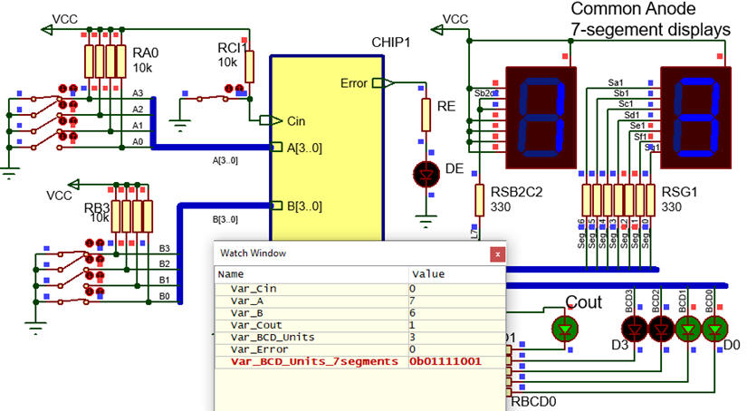 |
| Fig. 13. The circuit in "run" mode while monitoring RAM variables in the "watch" window. |
5. Report
Having solved this introductory project, also means that you are able to answer most of the questions listed here.
Do you become fully aware now on how designing an example also means learning the "theory" ?:
Having solved the project in paper, you are always in time to publish (as an option) your project report using a word processor: scanned figures, file listings, docx , pptx, or any other resources.
Remember that in class you'll be required to explain any section of your project individually or in group.
Follow this rubric for writing reports.
6. Prototyping
Example 1: Board Picdem2+. Target microcontroller: PIC18F4520. Tools: MPLAB X + XC8 + Proteus
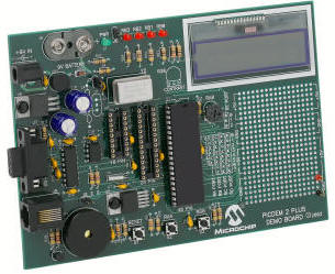 |
Fig. 14. PICDEM2+ board to be used with a PIC18F4520 chip. Expansion connectors or prototyping area can be used to connect switches and LED. |
Example 2: Board Explorer 8. Target microcontroller: PIC18F4520. Tools: MPLAB X + XC8 + Proteus
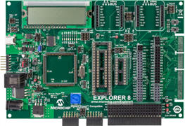 |
Fig. 15. Explorer 8 board to be used PIC18F4520 chip. The same code as in the previous example. Expansion connectors can be used to connect buttons and LED. |
Example 3 optional, beyond the CSD learning objectives. Board Explorer 8. Target microcontroller: PIC18F46K22. Tools: MPLAB X + XC8 + MCC + Proteus. Project: Intro_lab
To take full advantage of this board the programming environment requires MCC (MPLAB Code Configurator) application embedded in MPLAB X. The chip must also be upgraded for instance to PIC18F46K22, which is also available in Proteus.
This is an introductory project Intro_lab.pdsprj to guide you on the use of MCC to specify hardware and peripherals. The application program Intro_lab.X.zip is organised in multiple c files. Unzip and copy the full directory at location:
C:\CSD\P9\Intro_lab\(files)
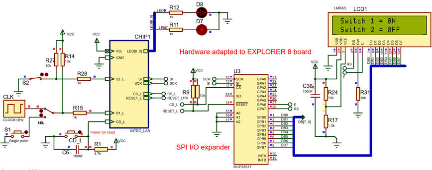 |
Fig. 16. This application can be used as a seed project to copy and adapt, no need to start from scratch. The full tutorial application that exemplifies several features of the hardware in Explorer 8 is available from Microchip product page. |
Optional project:
EXE key (interrupts, edge detection)
1. Specifications
A good example to see how the interrupt mechanism for detecting signal edges works is for instance: modify the design phase #1 (Adder_BCD_1digit) above so that the truth table is calculated only when EXE pushbutton is pressed. This means that even if the input operands are changed, only after clicking EXE the results will be displayed.
 |
|
Fig. 1. Adder_BCD_1digit circuit modified with EXE input. |
Some ideas to organise the project:
- Copy Adder_BCD_1digit.pdsprj to the new project folder and adapt the hardware circuit from P9. Project locations and file names:
C:\CSD\P9\Adder_BCD_1digit_EXE\(files)
- Study the INT0 mechanism and how it is configured in init_system(). Consider hardware flag INT0F and its software variable: var_EXE_flag.
- Modify the software flowchart so that truth_table() is executed only once var_EXE_flag is set.
- Write the software source file Adder_BCD_1digit.c. Start an MPLABX - XC8 project targeted to the PIC18F4520 chip.
- Start compiling and testing (debugging) interactively watching variables and using step-by-step execution.
- How long does it take to execute the ISR()?
| Home Term 24/25-Q1 Contact Products Electronic devices and companies Software Books Magazines Instruments DEE Library EETAC DEEL |

|
|
| Web activa des de 09/2001, @ F. J. Robert, J. Jordana. Web editat amb Microsoft Expression Web 4. El contingut és un complement als materials d'estudi del curs Circuits i Sistemes Digitals disponibles al campus digital Atenea. Llicència:Reconeixement 4.0 Internacional de Creative Commons |