Laboratory |
Laboratory 9: microcontrollers. basic digital I/O. Software organisation [P9] IDE and mC tools: C language, break points, step by step mode, watch windows, etc. |
[28/11] |
|
Individual post lab assignment PLA9 to be discussed next Lab10. Study and execute in your computer this lab tutorial before attempting to solve the post lab assignment. |
| 1. Specifications | Planning | Dev. & test | Prototype | report |
3.4.1. Specifications
Solve a combinational circuit using a PIC18F4520 microcontroller.
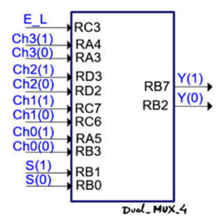
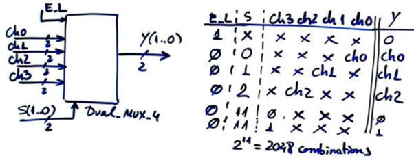
Our goal is to design again a dual 4-channel multiplexer (Dual_MUX_4) like 74HCT153 that was already solved in P2-P3 using plan A, B and C2. Symbol, truth table and timing diagram in Fig. 1 as it was described in Chapter 1 project Dual_MUX_4.
 |
|
Fig. 1. Symbol and truth table. |
This time the circuit will be based on a microcontroller (μC) PIC18F4520. Input and output signals have been distributed in different ports of the microcontroller so that you can practise on software organisation and on how to read and write individual pins.
 |
|
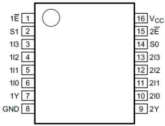
| Fig. 2. This is the chip 74HCT153 that is taken as a reference and the symbol of the Dual_MUX_4. The symbol includes the port pins of the microcontroller where the input and output signals are connected. |
|
| Specifications | 2. Planning | Dev. & test | Prototype | report |
3.4.2. Planning
Let us use the target mC chip: PIC18F4520 in Fig. 3. Target chip can be any other microcontroller or Arduino (ATmega328P). Our aim is to practise with digital inputs and outputs. Thus, several pin options will be proposed for reading inputs and writing outputs.
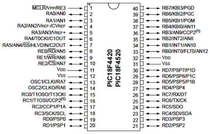 |
Fig. 3. Pin out diagram of 40-pin PDIP PIC18F4520 μC. |
A) Planning hardware
3.4.2.1. Hardware schematic
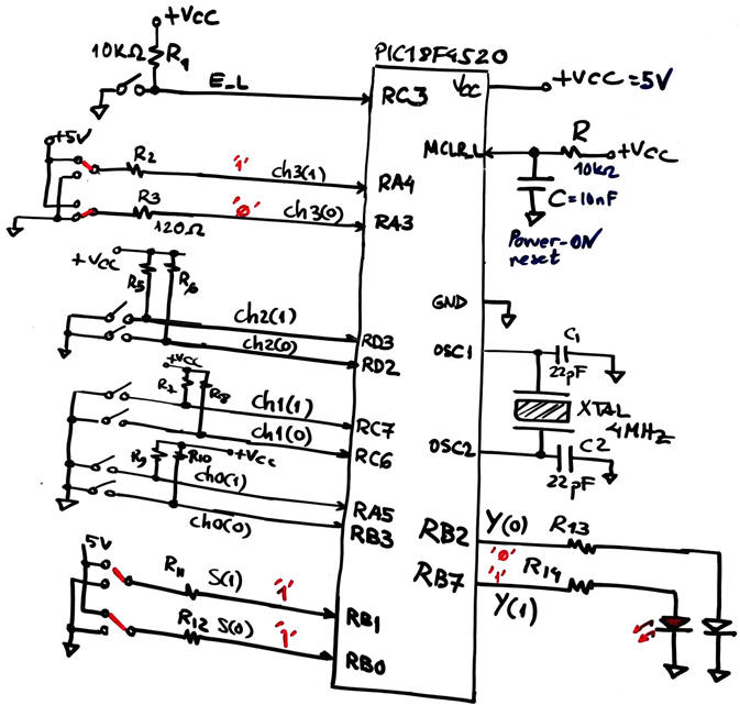
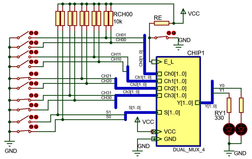
Hardware circuits and port connections in Fig. 4. Here the signals are connected to different ports in order to practise reading (polling) and writing digital pins using bitwise logic operations.
 |
|
Fig. 4. Hardware schematic using switches and LED. |
B) Planning software
3.4.2.2. Software organisation: setup, main loop
3.4.2.2.1. Hardware-software diagram and software organisation
3.4.2.2.2. RAM variables
3.4.2.2.3. init_system(): I/O port pin configuration data direction register TRIS.
3.4.2.2.4. read_inputs()
3.4.2.2.5. truth_table(), behavioural description, algorithm
3.4.2.2.6. write_outputs()
Fig. 5 shows the general proposal in CSD for organising the software, this is our coding style to make designing circuits simple and repeatable, each function has a specific task to solve.
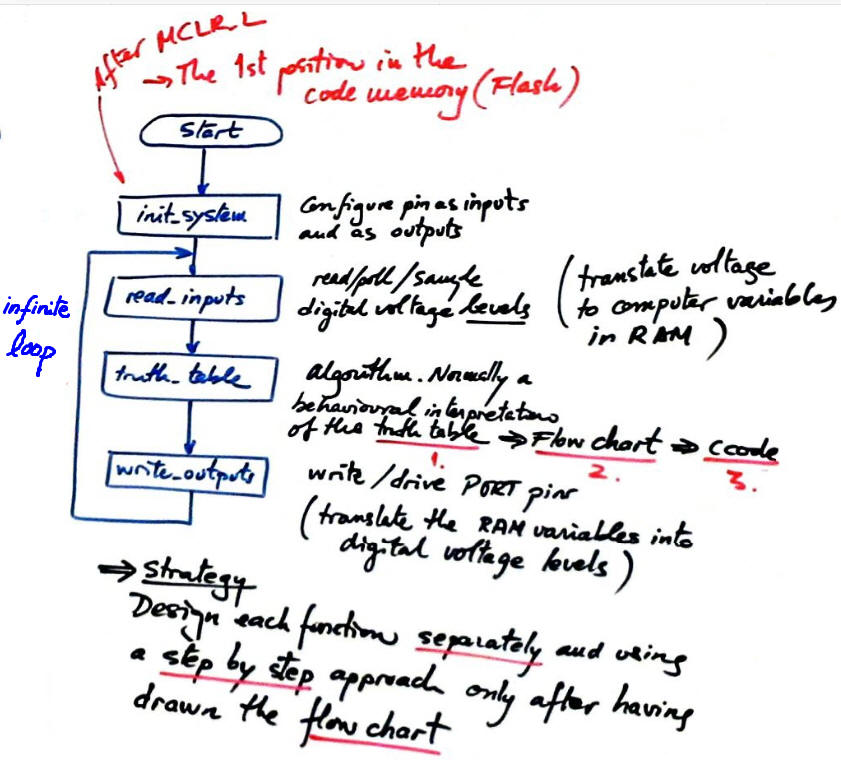 |
Fig. 5. Software organisation to poll inputs from port pins, to organise the RAM variables, to calculate the truth table and to send back the generated variables to output pins in an infinite loop. |
Here in Fig. 6 we include a new tool: the hardware-software diagram that allows us to visualise how the functions are related and what information are processing.
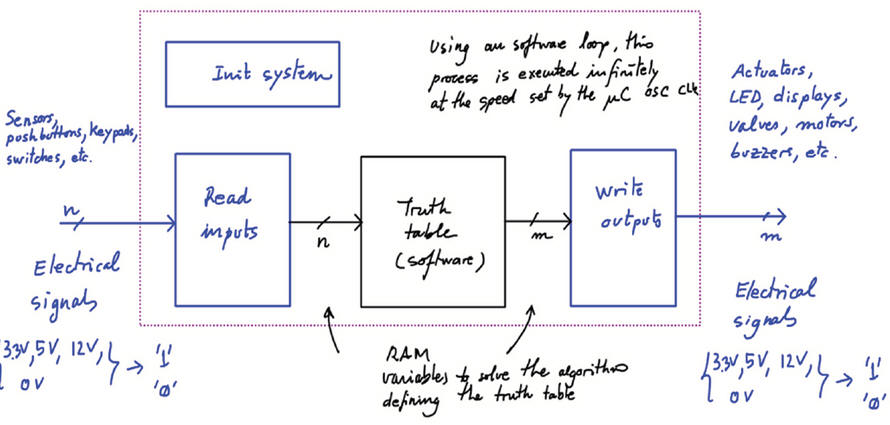 |
Fig 6. The new conceptual representation tool: hardware-software diagram. |
In Fig. 7 there is the list of RAM variables used.
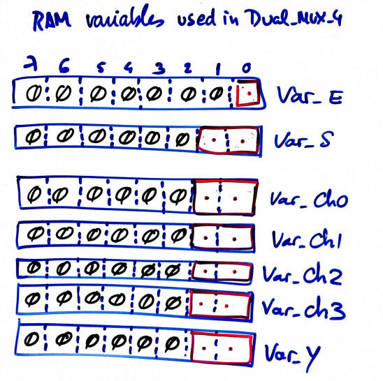 |
Fig. 7. Example of some convenient variables "Var" that will allow the processing of information in truth_table() independently of the microcontroller hardware. Program variables will be stored in RAM memory addresses and so, they are volatile. Accordingly to our programming style to assign a byte per variable, seven RAM bytes are required, and some more are required for partial results, such as var_buff. In our simple programs RAM variables will be global (accessible from anywhere in the code), but var_buff for saving partial results within a function may be local. |
Hardware interface functions. Firstly, init_system() to set pin directions as in Fig. 8. Read notes on how TRIS register bits configures a pin to be an input or an output using tri-state gates. All unused pins will be configured as outputs by default.
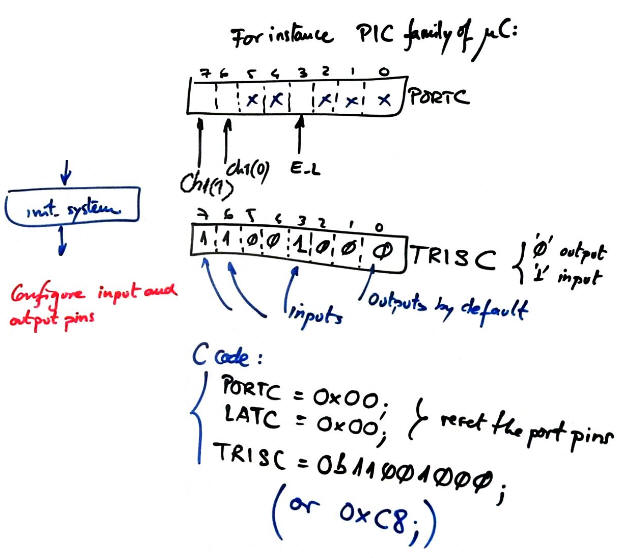 |
Fig. 8. Init_system() to set pin directions. |
Secondly, read_inputs() as represented in Fig. 9 on how to read a digital input rec. for reading/polling/capturing inputs voltage values.
And this is another rec. on how to start a new project from this tutorial following the step by step strategy (one line of code at a time).
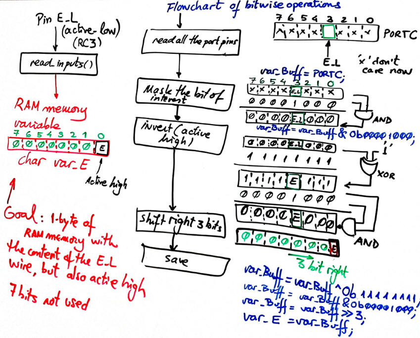 |
| Fig. 9. Read/poll/capture/acquire inputs. The concept "sampled inputs" is better applied in contexts where there is a CLK signal as it was for synchronous systems in Chapter 2. |
And thirdly write_outputs() in Fig. 10 on how to write a given pin into a port while preserving the information of the other pins of no interest. The idea is that even if the pins of no interest are not connected, they may be used in a future enhancement of the application.
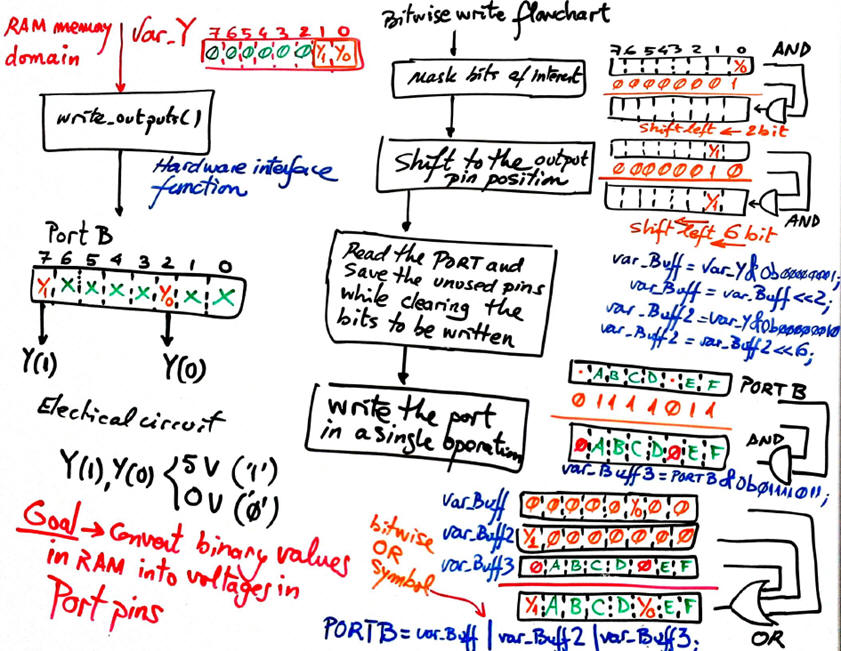 |
| Fig. 10. The concept of writing RAM variable values in a specific pin of a port using a single write-port operation and preserving at the same time the unused pins for future modifications. |
Conveniently, It is time to interpret the truth table in Fig. 11 (or algorithm or processing function) in a behavioural way exactly as we did in Dual_MUX_4 plan B. Flowchart is translated to C code instead of VHDL. The advantage of such code organisation based on hardware-independent functions is that flowchart is translated to C for any microcontroller, to ino for Arduino or python for Raspberry Pi.
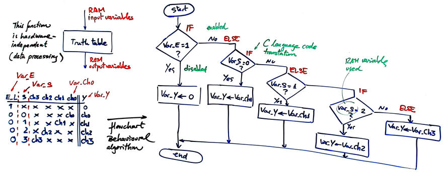 |
| Fig. 11. Example of behavioural interpretation of the truth table. |
Thus, what you see here is a powerful concept: all software algorithms are hardware-independent, meaning that they rely completely in RAM variables being totally compatible between hardware computer platforms. If the technology has to change only the hardware-dependent functions must be adapted, and this is what hardware drivers do in computer organisation. This concept is explained in Fig. 12.
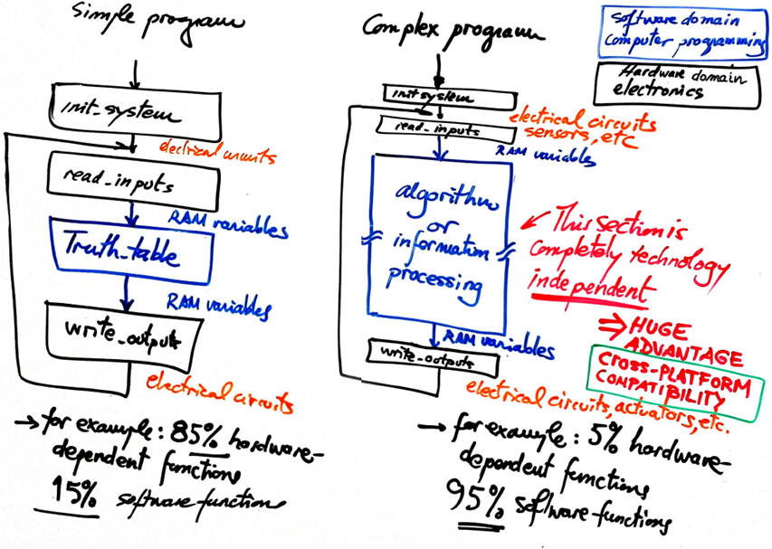 |
| Fig. 12. Software organisation from the compatibility point of view. |
Important remark: As you have seen, and also from your experience in Chapters 1 and 2, do not write C code without having sketched firstly hardware schematics and program flowcharts. Because as in VHDL, C code is again a simple translation of the information already studied and fully annotated in paper. Therefore, the C code of a given project, even if it is correct, has no value and is not assessed unless handed in accompanied by the corresponding work in paper.
Project location:
C:\CSD\P9\Dual_MUX_4\(files)
Target μC chip: PIC18F4520. Target prototyping board: PICDEM2 plus.
| Specifications | Planning | 3. Dev. & 4. test | Prototype | report |
3.4.3. Development and testing
Learning how to develop and test interactively microcontroller projects
|
Key indications for saving study
time and learning these materials correctly:
Step-by-step tactical approach for developing and testing the project:
Read one input at a time and run to watch that the voltage
value is correctly digitalised as a valid digital value in
RAM memory. Write one output at a time
and run to check that your code is correct to light LED
connected at output pins. Solve the truth
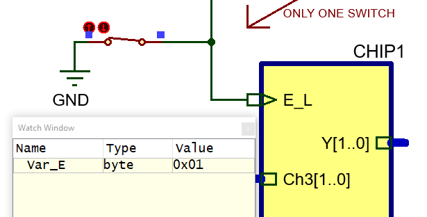
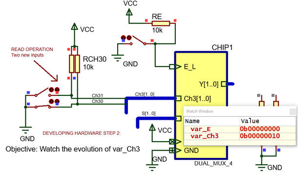
table algorithm and run. The three functions are totally independent and the order in which they are coded is not important. Or alternatively, the development and testing of the three functions can be assignment to three students working in the same group. Reading inputs Step #1): Hardware. Consider the circuit with oscillator, reset, and only the pin E_L connected to pin RC3.This is the file Dual_MUX_4.pdsprj. Save it at the working directory. Software. Comment or delete all the code that is not referred to CE_L. Translate the Fig 9 flowchart into C code. This is the file Dual_MUX_4.c. Save it at the working directory. Start a new project for a PIC18F4520 and compile. Run and add the watch window to monitor the RAM value var_E.
Step #2): Hardware. Add a new input in the schematic, for instance Ch3(1..0) Dual_MUX_4.pdsprj. Software. Translate to C the planned flowchart and add it to the previous program Dual_MUX_4.c.
Repeat new steps to complete all inputs. |
||||
|
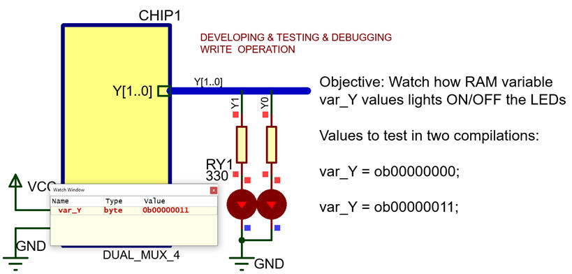
Writing outputs. #1): Hardware. Add a pair of LED to visualise Y(1..0). This is the file Dual_MUX_4.pdsprj. Save it at the working directory.Software. Comment or delete all the code that is not referred to var_Y. Translate the Fig 10 flowchart into C code. This is the file Dual_MUX_4.c. Save it at the working directory. Start a new project for a PIC18F4520 and compile. Run and add the watch window to monitor the RAM value var_Y when at the same time you check that the LED are lighting correctly.
Add similar writing steps in projects with more outputs. |
||||
|
Truth table Hardware. Consider the circuit only with oscillator and reset. This is the file Dual_MUX_4.pdsprj. Save it at the working directory.Software. Variables read (as outputs from read_inputs() function will be simulated by fixed values in successive compilations. Translate the Fig 11 flowchart into C code. This is the file Dual_MUX_4.c. Save it at the working directory. Start a new project for a PIC18F4520 and compile. Run and add the watch window to monitor the RAM values related to the truth table execution.
|
Initial steps to start a new project in MPLABX for target PIC18F4520, compile and simulate rec.
3.4.3.1. Proteus schematic capture: pdsprj file
A) Developing hardware
-
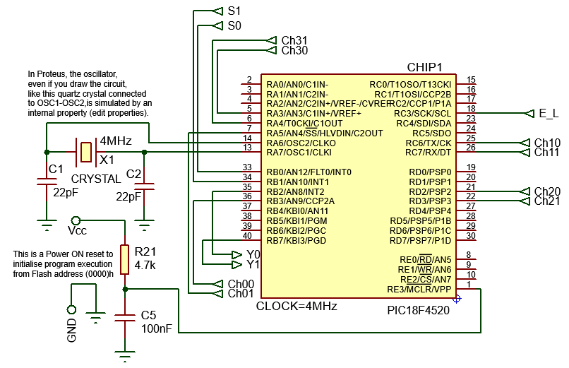
Target μC: PIC18F4520 --> This is the complete circuit captured in Proteus: Dual_MUX_4.pdsprj
 |
 |
|
Fig. 13. The block to be designed and the microcontroller connections captured in Proteus-VSM. It is better to use switches (or push-buttons) and resistors to generate inputs instead of ideal LOGICSTATE values. These ideal simulation values impose voltages in port pins that are not correctly handled by port circuitry and TRIS register cannot program correctly pin directions. |
3.4.3.2. MPLABX project for PIC18F4520: C source file
3.4.3.3. Project compilation and chip configuration files: hex, cof
B) Developing software
Run the integrated development environment IDE MPLAB X (with the included XC8 C compiler) and start a new project.
-
Project folder C:\CSD\P9\Dual_MUX_4\(files)
-
Target μC: PIC18F4520 --> This is the complete C source code translation to be compiled: Dual_MUX_4.c
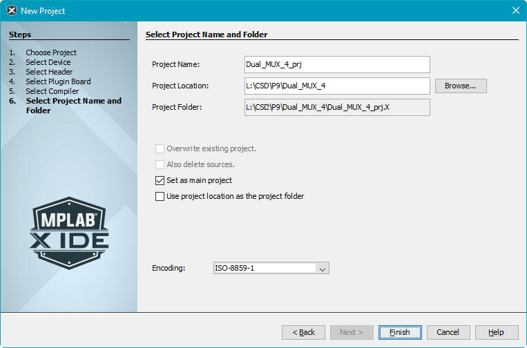 |
Fig. 14. Project name and folder. |
Compile the C code, generate the HEX and the COF chip configuration files, and attach the latest to the microcontroller properties window for debugging purposes.
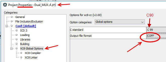 |
| Fig. 15. This is the way to configure project properties so that the COF file to be used with Proteus is generated. |
Compilation results, RAM and ROM memory used
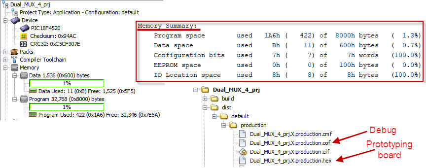 |
| Fig. 16. Compilation results, outputs files and memory used (11 bytes of RAM). |
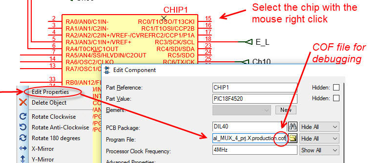 |
| Fig. 17. This is the way to attach in Proteus the hex or the cof to the chip properties, which in the simulator is equivalent to downloading the configuration code to the real chip populating the prototyping board. |
3.4.3.4. Proteus simulation and testing. Step by step debugging, watch variables window
C) Step-by-step testing
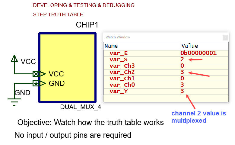
Run Proteus and test the circuit using step by step, break points and the watch window tools, as shown in Fig. 18.
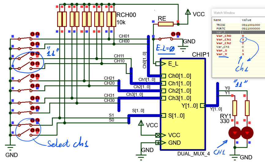 |
|
Fig. 18. Example of "run" simulation that includes a watch windows for monitoring variables of interest. |
3.4.3.5. Software execution time
D) execution speed measurements
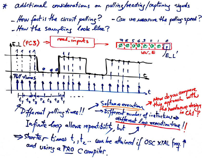
In Fig. 19 there are some questions of interest related to this initial program and process of reading inputs. What are the advantages and drawbacks?
 |
|
Fig. 19. Final slide with some questions and remarks. |
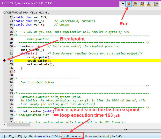
For example: how to measure the time that the microcontroller takes to execute the loop? As shown in Fig. 20, you can use a single breakpoint located anywhere in the loop and click run several times. The time elapsed since the last break is the loop execution time.
 |
|
Fig. 20. Measurement of the loop execution time using breakpoints. |
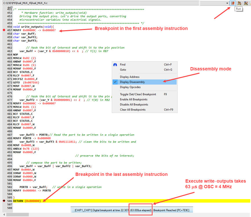
In the same way, using two breakpoints you can measure how long does it take to execute some instructions. Fig. 21 show the execution time of the write_ouputs() function. And, as usual, the speed limit is on the technology and also in the tradeoff with the dynamic power consumption (see L4.3 to review these concepts on how gate switching speed is related to dynamic power consumption).
 |
|
Fig. 21. Measurement of the loop execution time using breakpoints. |
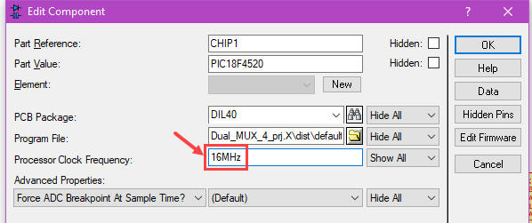
The microcontroller crystal oscillator frequency is a fundamental parameter. A 16 MHz executes assembly instructions four times faster than a 4 MHz crystal. You can adjust this parameter in the chip's edit properties window.
 |
|
Fig. 22. Setting the simulator's OSC microcontroller frequency. |
See how long does it take to execute an assembly instruction. Most of the instructions takes four OSC periods TOSC to execute.
| Specifications | Planning | Dev. & Test | 5. Prototype | Report |
3.4.5. Prototyping and laboratory experimentation
3.4.5.1. Chip programmer and program download
3.4.5.2. In-circuit debugging
3.4.5.3. Measurements and characterisation
Use training boards and perform laboratory measurements to verify how the circuit works. We can design a basic board for PIC18F mC such CSD_PICstick.
| Specifications | Planning | Dev. & Test | Prototype | 6. Report |
Follow this rubric for writing reports.
About code listings and ideas on how to print coloured code.
Optional. The same example (hardware and software source C code) for other microcontrollers:
-
ATmega8535 --> Dual_MUX_4 (zip)
-
PIC16F877A --> Dual_MUX_4 (zip)


