|
|
Bachelor's Degree in Telecommunications Systems and in Network Engineering |
|
P1: Design of simple circuits based on logic gates using plan A |
| Resources in lectures and labs: | L1.4, L1.5, L1.6, Lab1.1, Lab1.2 | Project | objectives |
Highlighted tutorial design project: Circuit_C
| 1. Specifications | Planning | Developing | Testing | Report | Prototype |
Objective design. From Circuit_C truth table in Fig. 1, invent equivalent circuits using logic gates (plan A).
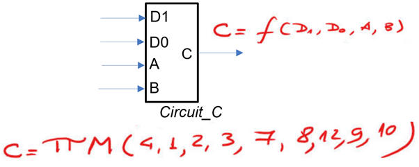 |
Fig. 1. Circuit_C symbol and truth table. |
For example:
Circuit_C1 - Using canonical equations (maxterms)
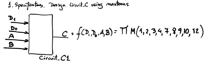 |
Fig. 2 |
Circuit_C2 - Using canonical equations (minterms)
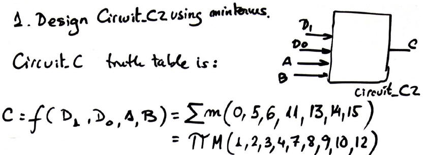 |
Fig. 3 |
Circuit_C3 - Using minimised equation sum of products (SoP) from minilog.exe (Karnaugh map application).
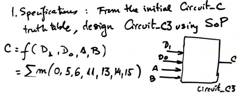 |
Fig. 4 |
Circuit_C4 - Using minimised equation product of sums (PoS) from minilog.exe.
Circuit_C5 - Transform the Circuit_C3 and build another version using only NAND gates.
Circuit_C6 - Transform the Circuit_C4 and build another version using only NOR gates.
Circuit_C7 - Transform the Circuit_C1 and build another version using only NAND gates.
Circuit_C8 - Transform the Circuit_C1 and build another version using only NOR gates.
Circuit_C9 - You can obtain a new circuit from any combination of equations. This is how Circuit_C was inferred.
Circuit_C10 - Transform the Circuit_C7 and build another version using only 2-input NAND.
Other design tutorials and assignments.
| Specifications | 2. Planning | Developing | Testing | Report | Prototype |
Planning means organising and discussing how to proceed to reach solutions. A flowchart of sequential operations will be convenient to explain what to do, how to do it and when. You can invent (or create, design, fabricate, imagine, envision, conceive, etc.) and test (or check, verify, validate, confirm, ensure, etc.) several circuits from specifications. Combinational circuits are specified from truth tables.
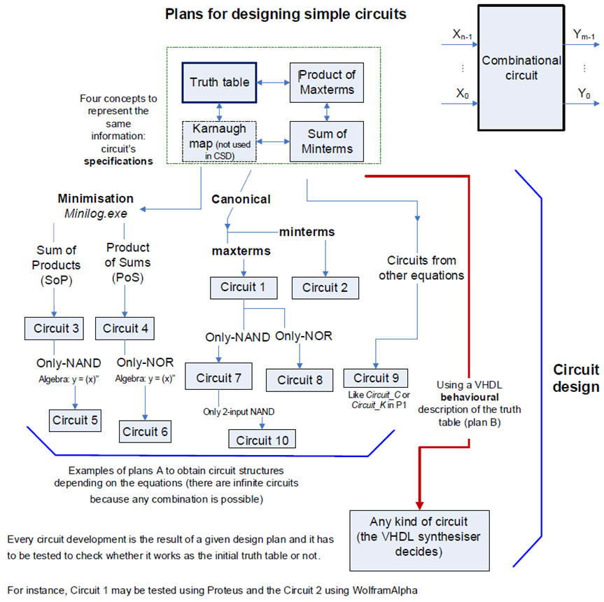 |
Fig. 5. Examples of circuits designed from initial specifications in truth table (Visio). |
In this introductory CSD course, considering VHDL language and electronic design automation (EDA) tools, three design strategies will be proposed: plan A: simple flat gate structures as shown in all ten examples in this page, plan B: high-level description and plan C2: hierarchical circuits.
This is the detailed list of strategies for inventing circuits using CSD plans.
In CSD we will imagine each circuit design as a project that follows the sequence in Fig. 3 usual in engineering.
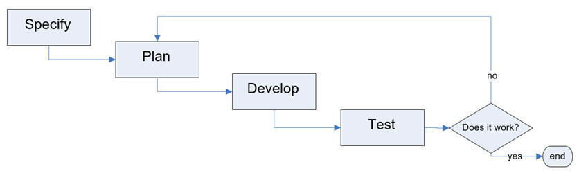 |
Fig. 6. Main operations in the process of designing projects. |
The final realisation will determine what tools to use in the design process. Sometimes will be possible to apply directly canonical equations and sometimes will be required minimising truth table logic functions.
Circuit_C1 - Using canonical equations (maxterms).
Project folder location:
C:\CSD\P1\Circuit_C\Circuit_C1\(files generated for this project based on maxterms)
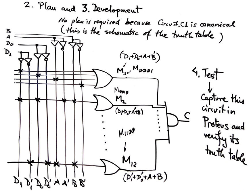 |
Fig. 7. Planning and building Circuit_C1. |
Circuit_C2 - Using canonical equations (minterms).
Project location:
C:\CSD\P1\Circuit_C\Circuit_C2\(files)
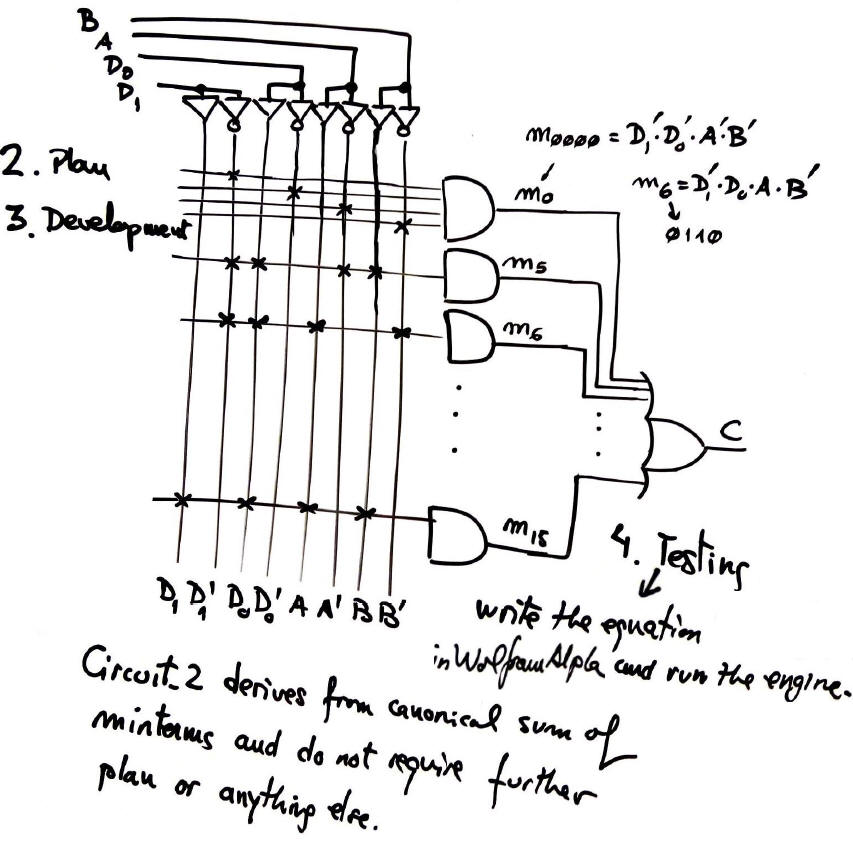 |
Fig. 8. Planning and building Circuit_C2 rec. |
Circuit_C3 - Using minimised equation sum of products (SoP) from minilog.exe (Karnaugh map application).
Project location:
C:\CSD\P1\Circuit_C\Circuit_C3\(files)
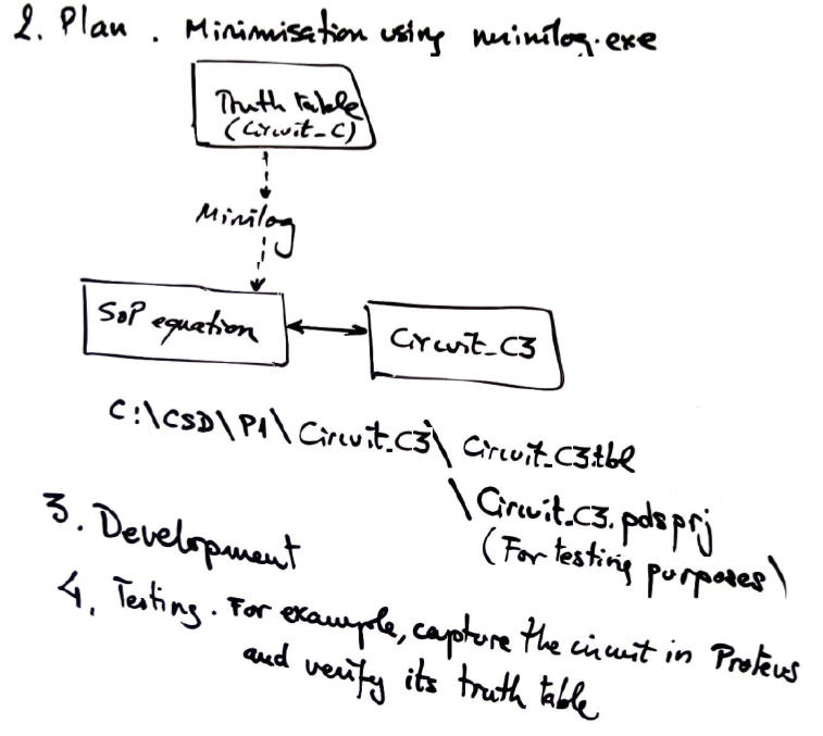 |
Fig. 9. Planning Circuit_C3. |
| Specifications | Planning | 3. Developing | Testing | Report | Prototype |
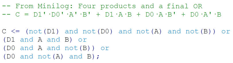
Minimised Circuit_C3 using SoP rec.
Truth table capture in minilog: Circuit_C3.tbl.
Circuit translation into VHDL: Circuit_C3.vhd.
 |
|
Fig. 10. Circuit_C3. Equation SoP from minilog and its translation to VHDL as architecture. |
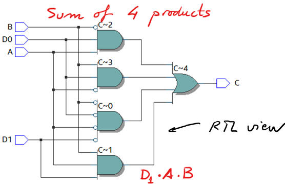 |
Fig. 11. RTL view. |
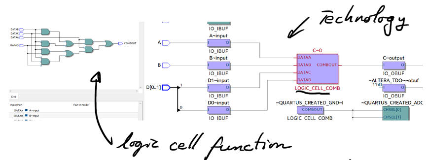 |
| Fig. 12. Technology view. |
| Specifications | Planning | Developing | 4. Testing | Report | Prototype |
Testing means to check or verify that the solution is correct and agrees with the initial specifications.
For instance, minimised Circuit_C3 can be synthesised using VHDL and tested using a testbench: Circuit_C3_tb.vhd
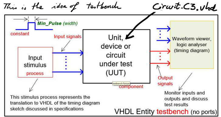 |
Fig. 13. Testbench fixture in VHDL. |
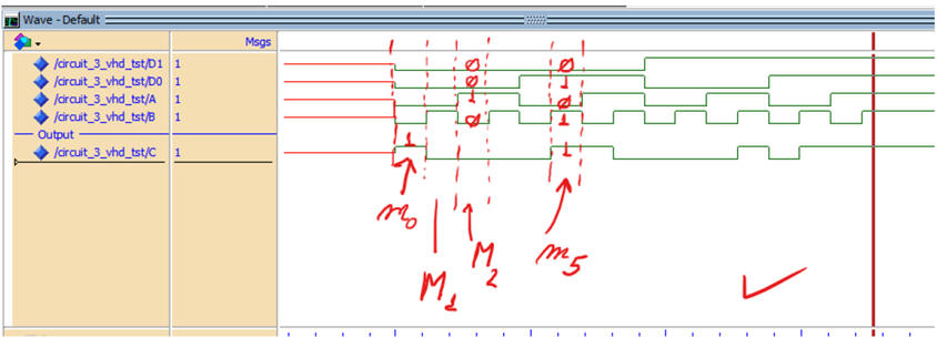 |
| Fig. 14. Simulation results from ModelSim waveforms |
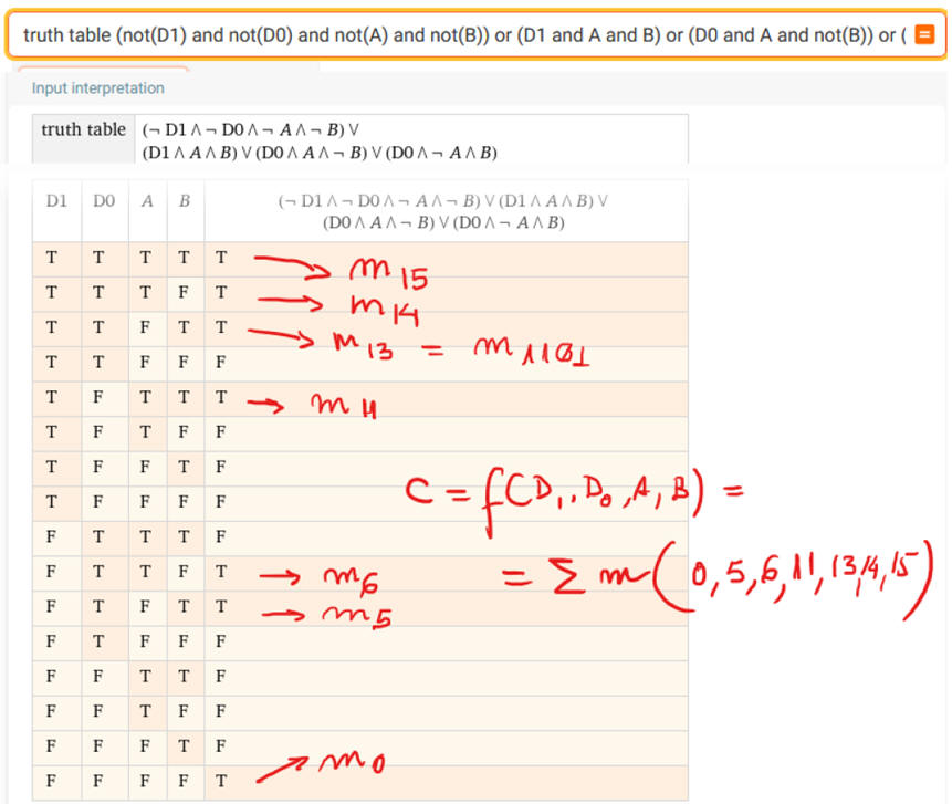 |
| Fig. 15. WolframAlpha verification. |
| Specifications | Planning | Developing | Testing | 5. Report | Prototype |
Follow this rubric for writing reports.
| Specifications | Planning | Developing | Testing | Report | 6. Prototype |
Building a prototype for Circuit_C is explained in Lab1.2 for Circuit_W using the Terasic DE10-Lite board.
| Home Term 24/25-Q1 Contact Products Electronic devices and companies Software Books Magazines Instruments DEE Library EETAC DEEL |

|
|
| Web activa des de 09/2001, @ F. J. Robert, J. Jordana. Web editat amb Microsoft Expression Web 4. El contingut és un complement als materials d'estudi del curs Circuits i Sistemes Digitals disponibles al campus digital Atenea. Llicència:Reconeixement 4.0 Internacional de Creative Commons |