|
|
Bachelor's Degree in Telecommunications Systems and in Network Engineering |
|
|
|
||
|
|
Mult_9bit plan B: single file behavioural VHDL design. |
|
|
|
||
Optional circuit in CSD: it is out of the scope of our introductory course and shown only for demonstration purposes.
1. Specifications
Design a multiplier for 9-bit radix-2 numbers using plan B. This means implementing the circuit's truth table as a behavioural high-level algorithm.
Fig. 1. Symbol, truth table and example of timing diagram. |
This is a Proteus example of hierarchical plan C2 8-bit multiplier Mult_8bit.pdsprj for radix-2 numbers build using a network of expandable 1-bit multiplier cells (Mult_1bit). This is for given an idea of the circuit complexity and the many resources (logic gates) used.
2. Planning
Project folder:
C:/CSD/P3/Mult_9bit/(files)
Translate the circuit in Fig. 4 to VHDL as usual: Int_Mult_9bit.vhd.
NOTE: See how this circuit and its behavioural design can be easily adapted to a different operand size. Quartus Prime will synthesise it efficiently attending the target chip resources. For instance Mult_8bit.vhd / Mult_8bit_tb.vhd.
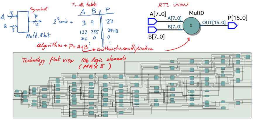 |
Fig. 7. RTL and technolgy implementation. |
4. Testing (functional simulation)t_8bit/img_mult_8bit_resut.jpg" />
Fig. 7. Multiplication results. hematic is represented in Fig. 7.
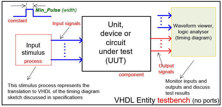 |
Fig. 7. Testbench VHDL schematic. |
Convert the initial timing diagram sketch into a VHDL testbench like in this file Int_Mult_9bit_tb.vhd writing input activity process and Min_Pulse constant in the template produced by the EDA tool. Use positive and negative numbers as inputs to the circuit.
Run the EDA VHDL simulator and demonstrate how the circuit works adding comments to the printed sheet of paper containing the waveforms.
|
|
Fig. 8. Example test with some input vectors A, B. |
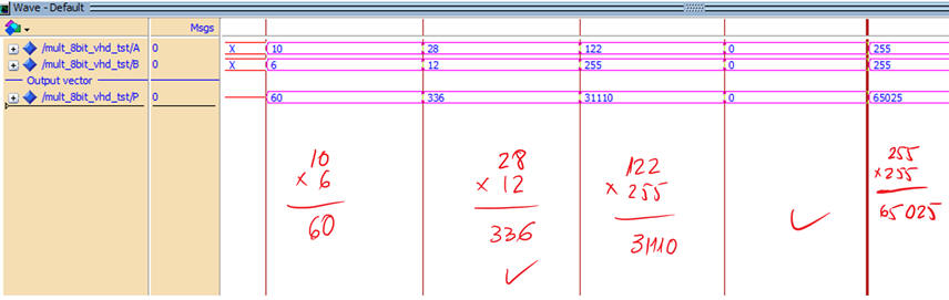 |
Fig. 7. 8-bit multiplication results. |
5. Testing (gate-level simulation)
VHDL design flow shows how gate-level simulations represent the 5th design step. The idea is to build a circuit prototype ready for laboratory experimentation and characterisation only when the circuit is fully tested.
Run a gate-level simulation to measure the propagation delay in a given transition.
|
|
Fig. 9. Example waveform for the Mult_9bit showing how a given input vector is computed over time generating wrong results until all signals have propagated through the circuit. In this transition it takes 10 ns to obtain the correct result. |
Use the timing analyser tool to determine worst-case scenario, and thus the maximum speed of comparison operations. In this example, the comparator can handle xxx millions of comparisons per second.
|
|
Fig. 10. Timing analyser spreadsheet. For a target chip MAX II the longest propagation time is tP = xxx ns. |
Repeat measurements for Intel Cyclone IV, and compare results.
Perform a simulation to show that the circuit cannot produce correct results when the Min_Pulse constant is less that the worst case delay.
6. Report
Follow this rubric for writing reports.
7. Prototyping
A prototype for the DE10-Lite board that used this component to perform integer multiplications is the ALU_9bit in Lab4.
| Home Term 23/24-Q2 Contact Products Electronic devices and companies Software Books Magazines Instruments DEE Library EETAC DEEL |

|
|
| Web activa des de 09/2001, @ F. J. Robert, J. Jordana. Web editat amb Microsoft Expression Web 4. El contingut és un complement als materials d'estudi del curs Circuits i Sistemes Digitals disponibles al campus digital Atenea. Llicència:Reconeixement 4.0 Internacional de Creative Commons |