|
|
Bachelor's Degree in Telecommunications Systems and in Network Engineering |
|
|
Laboratory |
Lab 4: propagation delay and speed. Adder_1bit - Adder_16bit RC - Adder_16bit CLA - Prototype [P4] Analysis of circuit's propagation delay using timing analyser and gate-level simulations |
[20/3] |
|
Individual post lab assignment PLA4 assignment to be discussed next Lab5. Study and execute this lab tutorial before attempting to solve your PLA. Learn how the new tools work running this tutorial projects fully solved in this page before venturing in your PLA. |
1.5.5.1. Gate-level simulation: propagation delay measurement
How to measure circuit's propagation time for a given target chip: post-synthesis model in VHDL (VHO file and its associated SDO/SDF delay file) and gate-level VHDL simulation.
1.5.5.2. Timing analyser spreadsheet tool
Measuring the worst-case scenario: longest propagation delay (tP).
1.5.5.3. Calculating circuit's maximum speed (fMAX).
In the lab we have some commercial CPLD and FPGA target chips where to synthesise our circuits. For instance:
| CPLD | FPGA | |
| Xilinx | XC2C256-TQ144 - 7 | Spartan-3E XC3S500E-FG320 |
| Intel | MAX II EPM2210F324C3 (option #1) | Cyclone IV EP4CE115F29C7 (option #2) |
| Lattice | ispMach4128V TQFP100 | MachXO |
NOTE: Quartus Prime do not generate delay files (sdo) for Intel MAX 10 devices, and thus we cannot practise gate-lelvel simulations in ModelSim for this family.
1. Specifications
Let us continue Adder_1bit based on MoM from Lab3 measuring propagation time of signals in a given transition and maximum speed of computing.
Two new tools will be presented:
-
(1) ModelSim gate-level simulations for measuring propagation delays in a given signal transition.
-
(2) Quartus Prime timing analyser for calculating the worst-case scenario (longest propagation delay).
The objective is to find what target chip is faster when implementing the same project Adder_1bit:
-
Option #1: MAXII device EPM2210F324C3
-
option #2: Cyclone IV EP4CE115F29C7
Firstly, we will solve the project for chip option #1 and annotate results. Secondly, keeping the same project, we will change the target chip to option #2 and annotate results. We will discuss solutions.
|
2. Planning |
||
|
3. Development |
||
|
4. Test: functional simulation |
The Adder_1bit specifications and also the three next sections #2 -#3 -#4 are already implemented in the previous Lab3. Our circuit is running correctly and we can visualise functional simulations. This, we can start a new Quartus Prime project copying the source VHDL files (Adder_bit.vhd, MUX_2.vhd, MUX_4.vhd) and the testbench files (Adder_1bit_tb.vhd, wave.do) from Lab3 to this new location:
C:\CSD\P4\Adder_1bit_MoM\(files)
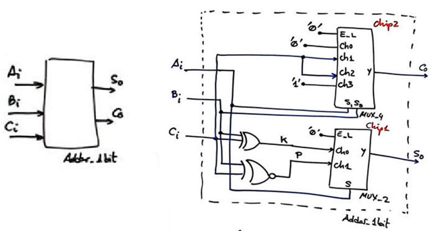 |
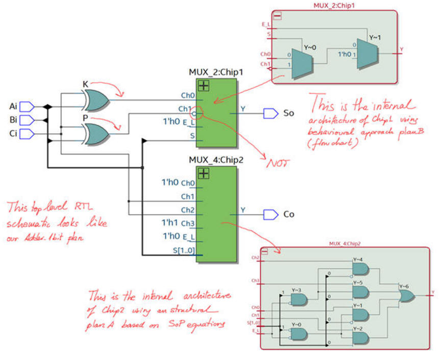
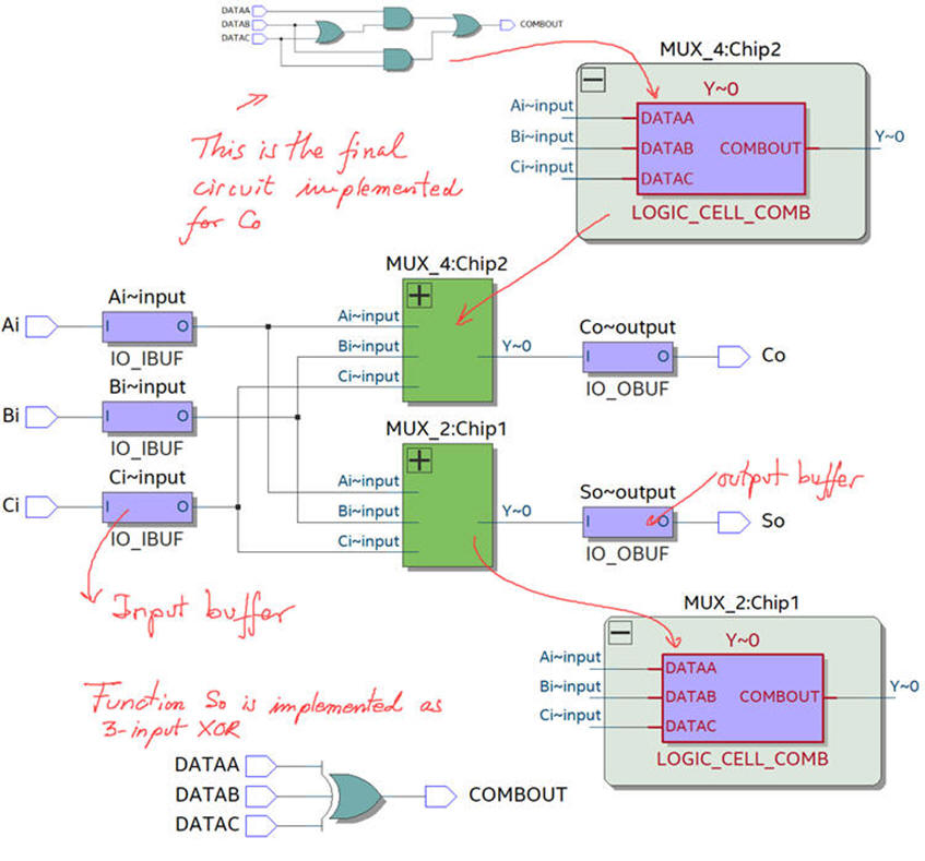
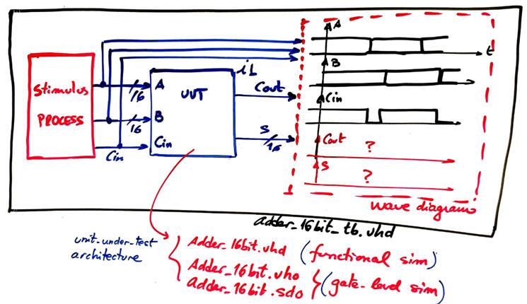
| Fig. 1. The plan for inventing the Adder_1bit is the same from LAB3. |
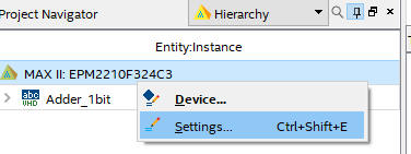
Select the option #1 MAX II target device and synthesise the circuit.
 |
Fig. 2. Plan C2 source files from Lab3. |
Be sure that you check the RTL and technology view as you did in Lab3 Fig. 6 and Fig. 7.
Check that you've got the same functional test results as in Lab3 and Fig. 10 when using the same VHDL testbench fixture Adder_1bit_tb.vhd. Use the same wave.do for setting up the signals oof interest in the wave diagram.
5. Test: gate-level simulation - timing analyser
Let us use the new tools that will allow us to characterise better the real circuit implemented in the FPGA. This is our tutorial on gate-level simulation and the timing analyser tool in case you needed it even before running this tutorial.
Set the following project parameters before re-synthesising your project and be able to generate the necessary VHO and SDO files for the target chip:
 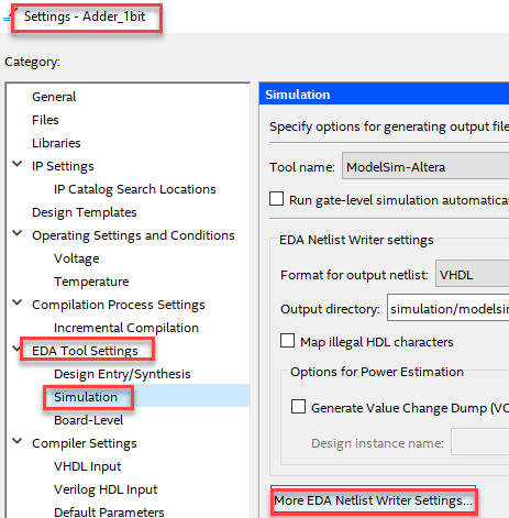 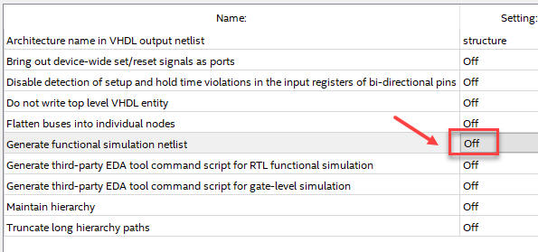 |
| Fig. 4. Parameters for letting Quartus Prime generate delay files. |
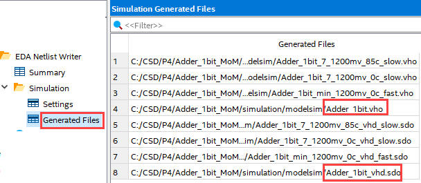
And now re-synthesise your project to generate in Quartus Prime the VHDL translation of the technology circuit (Adder_1bit.vho) and its delay file (Adder_1bit_vhd.sdo).
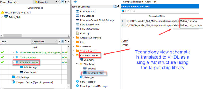 |
| Fig. 5. Indications for generating the VHDL technology circuit translation (vho) along with its delay file (sdo). |
Now you are ready for starting a ModelSim gate-level simulation for this flat circuit.
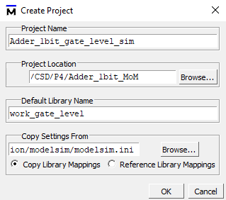 |
| Fig. 6. Create a new ModelSim project. |
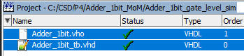
Add the same testbench that you also have copied from Lab3 to the new location:
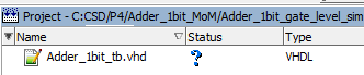  |
| Fig. 7. Add the same testbench and flat structure |
Compile all and check the project's integrity. Therefore, hierarchical structures formed by multiple VHDL files are replaced by a single flat VHO file to be tested using the same testbench.
 |
| Fig. 8. Check the project integrity. |
Start a new simulation paying attention this time to both "Design" and "SDF" tabs:
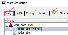 |
| Fig. 9. |
Attach the standard delay file to the region of interest:
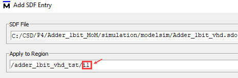 |
| Fig. 10. The region where to apply the SDO file is the instance i1 (the unit-under-test). |
Run and check that the full wave is the same as it was in functional simulations.
 |
| Fig. 11. Full view of the simulation results. |
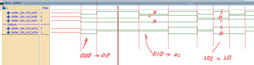
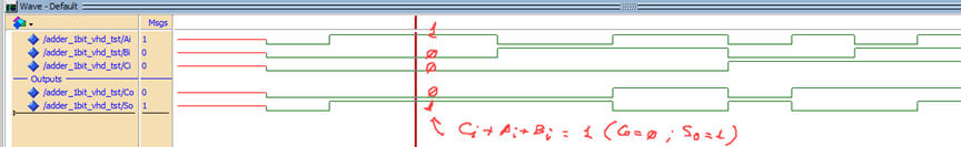
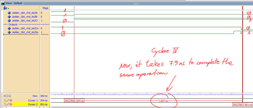
Zoom at a given signal transition to measure propagation delays using two cursors.
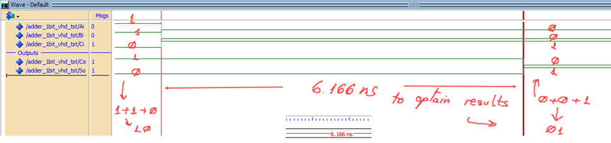 |
| Fig. 12. In this example transition, both outputs changes from "10" to "01" after 6.17 ns. |
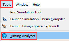
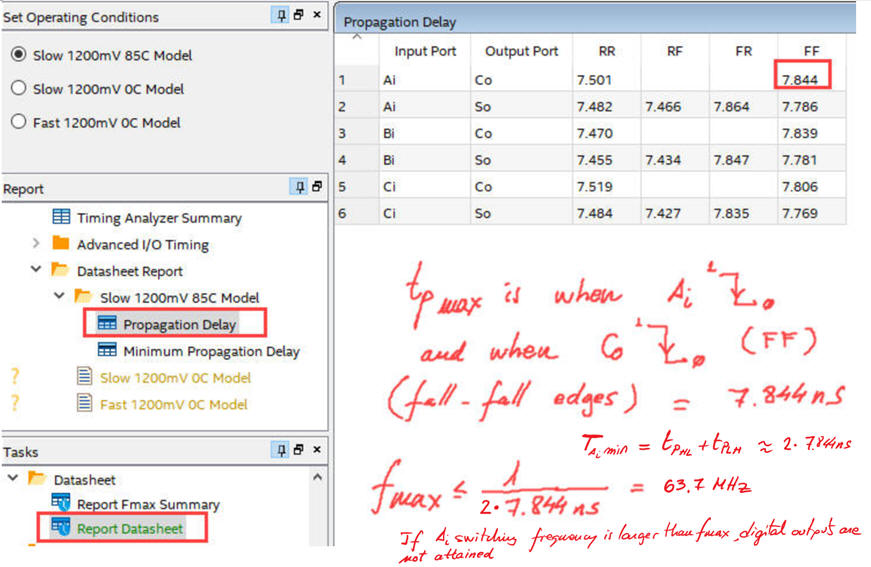
Go back to Quartus Prime to find the largest propagation delay using the timing analyser spreadsheet tool.
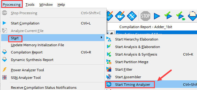 |
| Fig. 13. Starting processing the timing analyser tool. |
View results in the spreadsheet.
 |
| Fig. 14. View results using the timing analyser tool. |
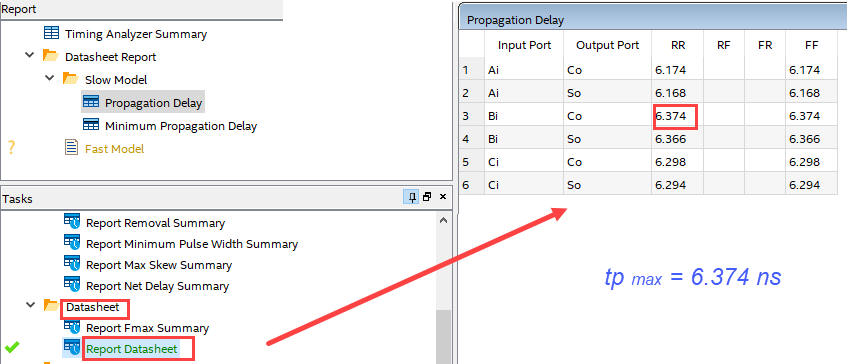 |
| Fig. 15. Spreadsheet from datasheet report. |
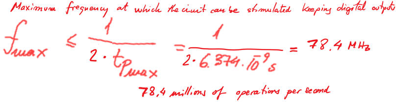
And so, calculate the maximum frequency of operation for this specific target chip MAX II (L4.3):
And now, you can redo the project (at the same location), changing the target chip and compare how this Addder_1bit is performing for an option #2 Cyclone IV target chip.
 |
| Fig. 16. Select a Cyclone IV device FPGA (Field Programmable Gate Array). |
Check that the files of interest are correctly generated for this new target chip. Indeed here you can find several simulation models (fast, slow, etc.):
 |
| Fig. 17. For this chip several delay models are generated. |
Recompile your ModelSim project and write down results:
 |
| Fig. 18. Cyclone IV measurements are slightly different at the same transition. |
And, using the timing analyser, we can observe a longer propagation delay than in MAX II.
 |
| Fig. 19. Cyclone IV measurements are slightly different at the same transition. |
And thus, the maximum frequency of operation for this Cyclone IV is slower that MAXII.
|
Laboratory |
Lab 4: circuit optimisation. Adder_1bit - Adder_16bit RC - Adder_16bit CLA [P4] Adder_16bit RC: comparing ripple-carry and carry-lookahead architectures |
[20/3] |
1.9.1.2. n-bit adders [L3.2]
1.9.1.2.1. Ripple-carry adder: Adder_4bit, Adder_8bit [Lab 3], Adder_16bit [Lab 4],(option #1)
1.9.1.2.2. Carry-lookahead adder: Adder_4bit, Adder_16bit [Lab 4], (option #2)
In the project above, you have seen how is implemented the same design in two target chips. Now we have in mind solving the same project Adder_16bit using two different architectures synthesised for the same target chip. Thus, learning basic concepts on circuit optimisation. You will observe what is the difference between ripple carry and carry-lookahead adders, which one is faster and why?
1. Specifications
Option #1: Design an Adder_16bit using ripple-carry technique (RC).
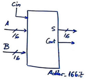 |
 |
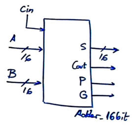
| Fig. 1. Symbol and example waveforms. |
|
Here we rely on the work done when designing the tutorial Adder_4bit ripple-carry (RC). Zero (Z) flag will not be implemented, it simply adds another level of gates and is not necessary for the purpose of comparing with the Adder_16bit CLA presented below as the third project in this lab session.
2. Planning
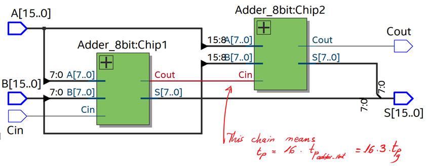
Fig 2 shows the ripple-carry architecture. Remember that we already have designed Adder_8bit component in Lab3 using the same carry chain strategy.
 |
| Fig. 2. Adder_16bit architecture. |
Project location:
C:\CSD\P4\Adder_16bit_RC\(files)
3. Development
Let us pick up a MAX II EPM2210F324C3 target chip.
VHDL file translation of the architecture in Fig. 2: Adder_16bit.vhd.
Components files: Adder_8bit.vhd , Adder_4bit.vhd and Adder_1bit.vhd (plan A or plan B) can be found in Lab3.
  |
| Fig. 3. RTL view and all the files requires in this design. |
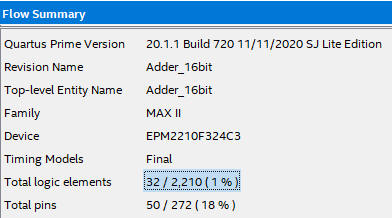
Technology view and project summary shows that only 32 logic elements are used for synthesising this project, saving much hardware with respect the CLA implementation below proposed in the next project.
 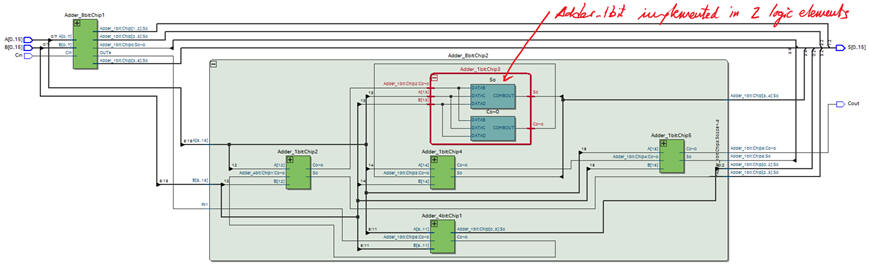 |
| Fig. 4.Technology view. Each Adder_1bit is implemented in two logic elements. To make it simple and comparable to classic technologies, we can imagine that the Adder_1bit is solved using 3 levels of gates. |
4. Test: functional simulation
This is the translation of the testbench fixture and some signal activity proposed in Fig. 1: Adder_16bit_tb.vhd. It can be used for both, functional and gate-level simulations.
 |
| Fig. 5. VHDL testbench fixture. The UUT is described as a hierarchical VHDL project when performing a functional simulation, and as a flat technology circuit when solving the gate-level simulation. |
The ideal functional results in this design step #4 must be identical for both projects of the same entity: ripple-carry and carry-lookahead Adder_16bit.
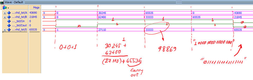 |
| Fig. 6. Functional simulation results. |
5. Gate-level simulation
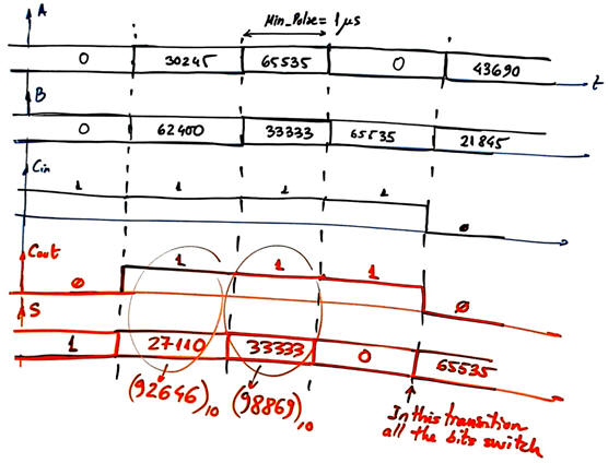
Running a gate-level simulation for this ripple-carry Adder_16bit, for instance, at the transition highlighted in Fig.1 where all bits have to change, we obtain an accumulated propagation delay of tP = 22.6 ns, practically doubling the one produced by the CLA adder in the project below.
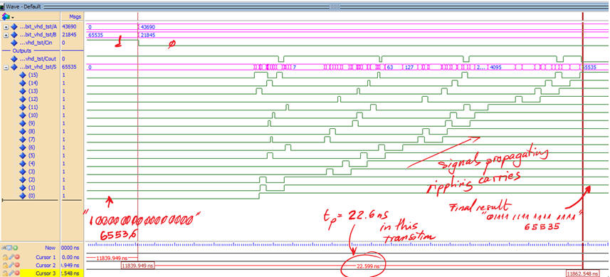 |
| Fig. 7. Gate-level simulation results at a particular transition. |
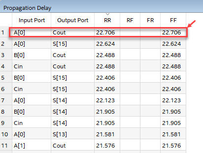
When running the timing analyser, the maximum delay occurs when driving A(0) and waiting results at Cout. This is tP= 22.7 ns, allowing a maximum frequency of operations of 22 Mops. (unsigned radix-2 16-bit millions operations per second).
 |
| Fig. 8. Timing analyser spreadsheet. |
Furthermore, at this point the answer to the question: which is the minimum value for Min_Pulse for experimentation in the laboratory becomes straightforward: Min_Pulse > tP. Min_Pulse smaller that the propagation delay of the circuit will imply that the circuit is going to be switching continuously, never being able to reach stable output values. We can verify that using this set of vectors Adder_16bit_tb.vhd as represented in Fig. 9 (Min_Pulse = 25 ns) and Fig. 10 (Min_Pulse = 20 ns).
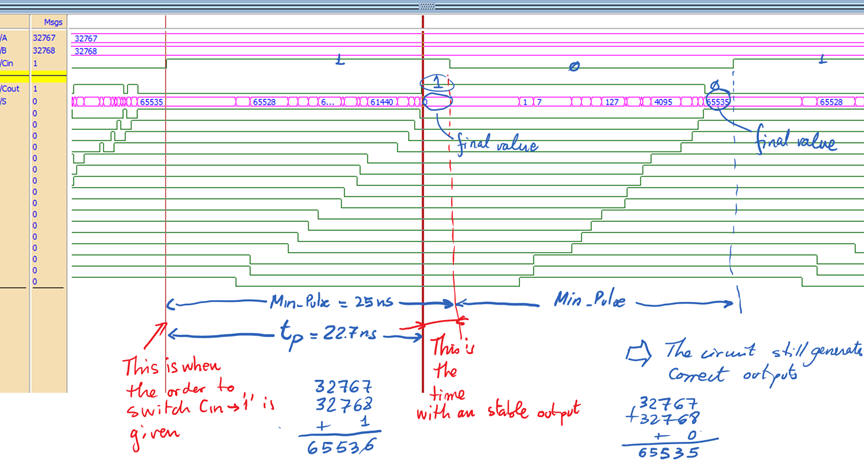 |
| Fig. 9. Min_Pulse is 25 ns, practically on the limit. |
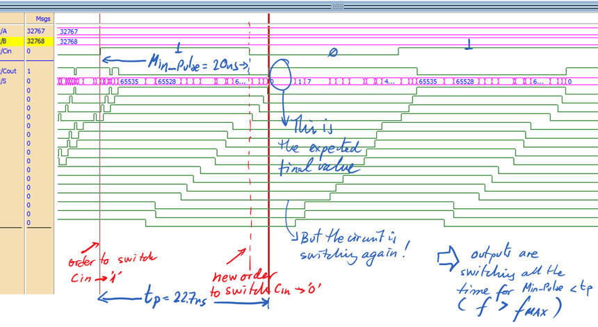 |
| Fig. 10. Min_Pulse is 20 ns < tP. Thus, the outputs never settles to a valid result. |
It is time to compare results with the new carry-lookahead design proposed in the next project.
6. Reporting
Follow this rubric for writing reports.
|
Laboratory |
Lab 4: circuit optimisation. Adder_1bit - Adder_16bit RC - Adder_16bit CLA [P4] Adder_16bit CLA: comparing ripple-carry and carry-lookahead architectures |
[20/3] |
1.9.1.2. n-bit adders
1.9.1.2.1. Ripple-carry adder: Adder_4bit, Adder_8bit [Lab 3], Adder_16bit [Lab 4], (option #1)
1.9.1.2.2. Carry-lookahead adder: Adder_4bit, Adder_16bit [Lab 4],(option #2)
Let us complete this lab tutorial considering the enhanced architecture based on carry-lookahead adders. You will observe what is the difference between ripple carry and carry-lookahead adders, which one is faster and why?
1. Specifications
Option #2: Design an Adder_16bit using the carry-lookahead (CLA) technique. The additional signals in this symbol P (propagator) and G (generator) are outputs required for chaining larger adders using the same CLA architecture.
The truth table and timing diagram are the same stated in Adder_4bit CLA considering now radix-2 numbers ranging up to 65535 = "1111111111111111".
 |
|
| Fig. 1. Symbol and waveforms. |
|
Here we rely on the work done when designing the tutorial Adder_4bit CLA. For instance, read in Wikipedia how an Adder_16bit works and how it is possible to calculate all carries beforehand. This reference also explains how to chain carry generators: Ercegovac, M., Lang, T., Moreno, J. H., "Introduction to Digital Systems", John Wiley & Sons, 1999). It includes slides: Chapter 10 is on arithmetic circuits.
2. Planning
Fig 2 shows the picture from Wikipedia that is adapted in CSD as Fig 3.
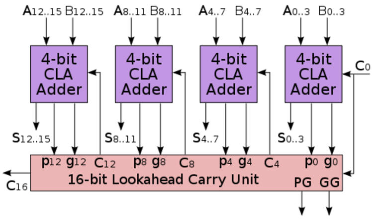 |
| Fig. 2. Adder_16bit architecture proposed in Wikipedia to be written in CSD as VHDL file. |
The Adder_16bit has the same structure than the circuit designed in Adder_4bit, as shown in Fig. 3.
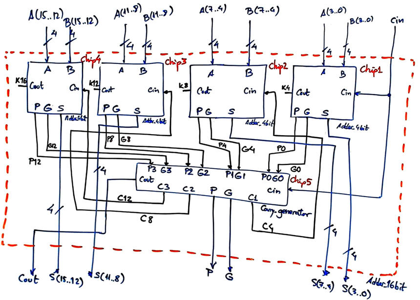 |
| Fig. 3. Planning the Adder_16bit. How many gate-levels are expected in this circuit? |
Project location:
C:\CSD\P4\Adder_16bit_CLA\(files)
3. Development
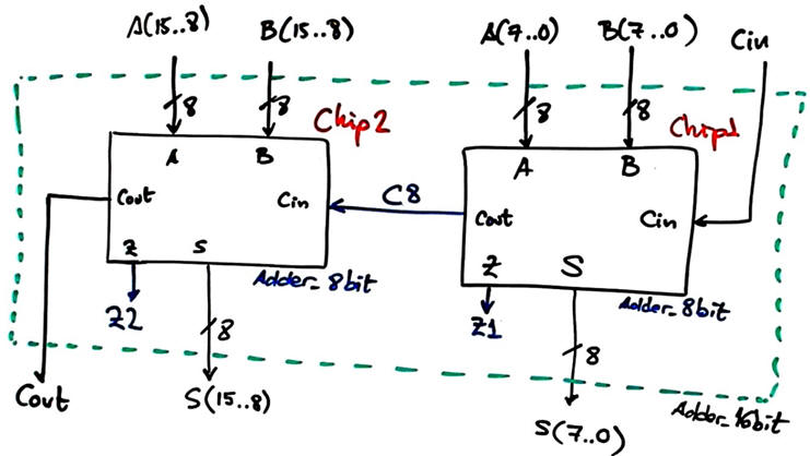
We will pick up the same Intel MAX II EPM2210F324C3 target chip. Thus, the same chip will implement the same entity but with two alternative architectures.
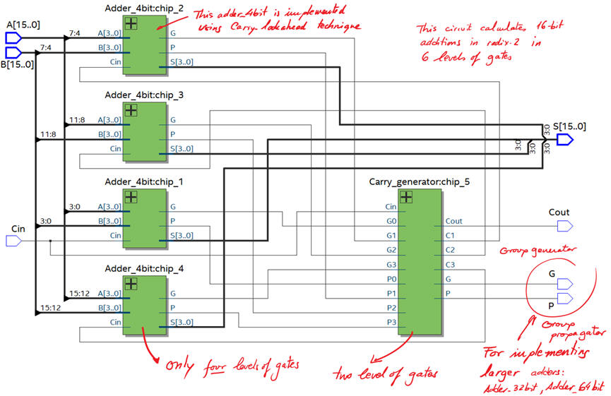
VHDL file translation of the architecture in Fig. 3: Adder_16bit.vhd.
Components Carry_generator.vhd and Adder_4bit.vhd can be found in tutorial Adder_4bit.
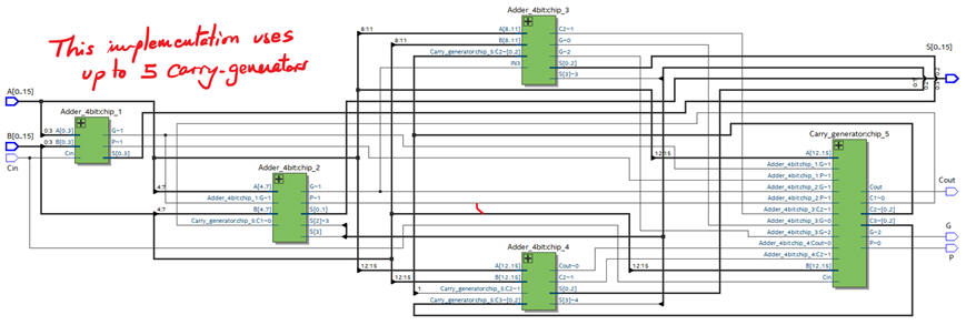
Start a VHDL synthesis project and observe the schematics. This time the architecture is far more complex, compromising up to 71 logic elements; more chip logic resources with the aim of obtaining a faster circuit.
 |
| Fig. 4. RTL view. |
The architecture uses up to five Carry_generator circuits organised in two levels (one carry_generator in each Adder_4bit module, and another one in the top entity). However, the largest number of logic gates levels is only six.
 |
| Fig. 5. Technology view. |
Chip planner tool allows us to map exactly where all the resources in use are located.
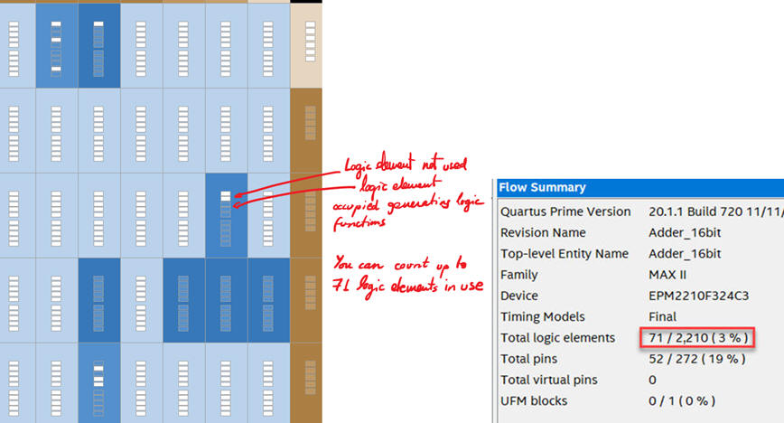 |
| Fig. 6. MAX II chip occupation from chip planner tool. |
4. Test: functional simulation
Now, it is time to test the synthesised circuit above. Thus, we can use the same VHDL fixture represented in the Fig. 5 of the previous project Adder_16bit RC.
Example of testbench Adder_16bit_tb.vhd from which to copy the stimulus signals. We are expecting the same ideal functional results represented in Fig. 7 when applying the same input vectors.
|
|
| Fig. 7. Functional results. |
5. Gate-level simulation
Now, when running a gate-level simulation at the same transition, a shorter propagation delay is obtained. Only 12.6 ns (saving 10 ns from the same design above based on ripple-carry).
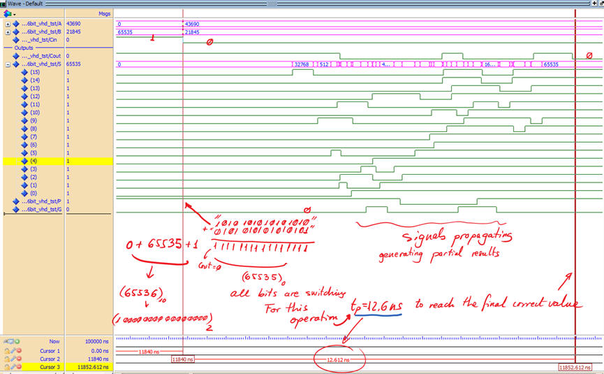 |
| Fig. 8. Gate-level simulation. |
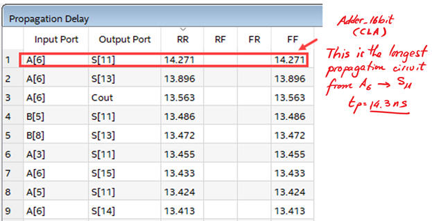
And, finally, measuring the longest propagation delay using the timer analyser tool, we can deduce the maximum circuit's speed. The longest signal path is established between input A(6) and output S(11), tP = 14.3 ns. This circuit is capable of performing 35 Mops. Thus, an improved architecture using more hardware (logic elements) generates a faster circuit.
The drawback is that the dynamic power consumption will be higher than the same circuit based on the RC technique. At this CSD introductory level, and from the perspective of classic technologies, we can say that the static power consumption will be larger because there are more gates connected to the power supply, and the dynamic power onsumption will also be larger because there are many more logic gates switching.
 |
| Fig. 9. Timing analyser spreadsheet showing CLA adder results. |
6. Reporting
Follow this rubric for writing reports.
Conclusions
These three projects have been used for learning new tools: gate-level simulation in ModelSim and Quartus Prime timing analyser, and for demonstrating how digital technologies, gate switching (operating speed) and logic resources (logic elements) are linked. We can imagine that when more resources are used the circuit is more power demanding. You can balance speed and power consumption choosing alternative designs.
-
The synthesis of a given architecture in a newer PLD chip will compute the same logic functions faster, because of shorter propagation delays.
-
Carry-lookahead architecture is much faster than ripple-carry, but it requires more circuits for generating and propagating carry signals in fewer gate-levels.
-
Ripple-carry circuits will be less power demanding that carry-lookahead circuits, because they are designed with less circuitry (logic gates, logic elements).
|
Laboratory |
Lab 4: propagation delay and speed. Adder_1bit - Adder_16bit RC - Adder_16bit CLA - Prototype [P4] ALU_9bit prototype using the DE10-Lite board |
[20/3] |
6. Prototyping
1. Specifications
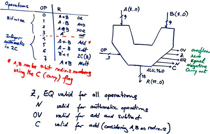
To practise with ALU we play with the prototype sketched in Fig. 1, an ALU_9bit capable of performing eight logic and aritmetic operations in a DE10-Lite board populated with an Intel MAX10 FPGA chip.
 |
|
Fig. 1. ALU_9bit symbol and projected operations. |
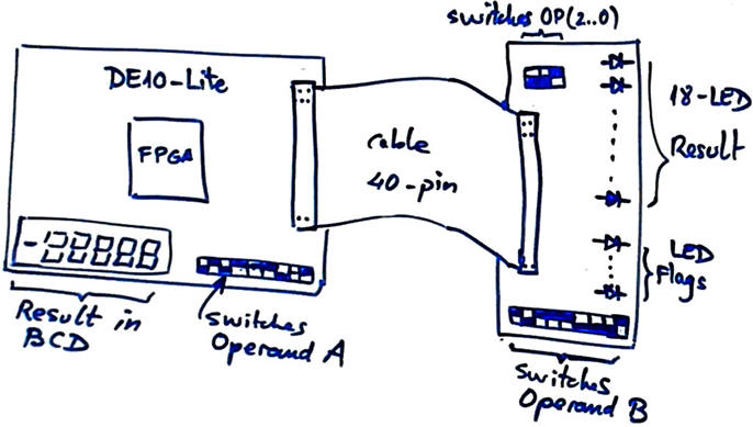
The DE10-Lite board switches can be used for inputting operand A. The six 7-segment displays can be used for representing results. In this way, we can populate a PCB connected through the 40-pin general purpose input-output connector GPIO for capturing the operand B, representing the full binary result in a LED array and lighting the flag indicators. In Chapter II, we can run the same application replacing the switches by a 16-key matrix keypad FSM as designed in P6 to input operands and operations sequentially as usual in a calculator.
 |
|
Fig. 2. DE10-Lite and PCB prototype. |
2. Planning
Plan C2 is required here to get an idea on the components involved and how they will be connected. To review the theory and how components work, we can get inspiration studying the circuits proposed in D1.18. Fig, 3 shows hierarchical schematic.
Logic operations are solve by gate blocks. The Adder_9bit used for both, adding and subtracting , is proposed in the final Annex A1. The integer multiplier is designed in this tutorial Int_Mult_9bit. Several multiplexers select the operands and additional logic circuits generate and enable status flags.
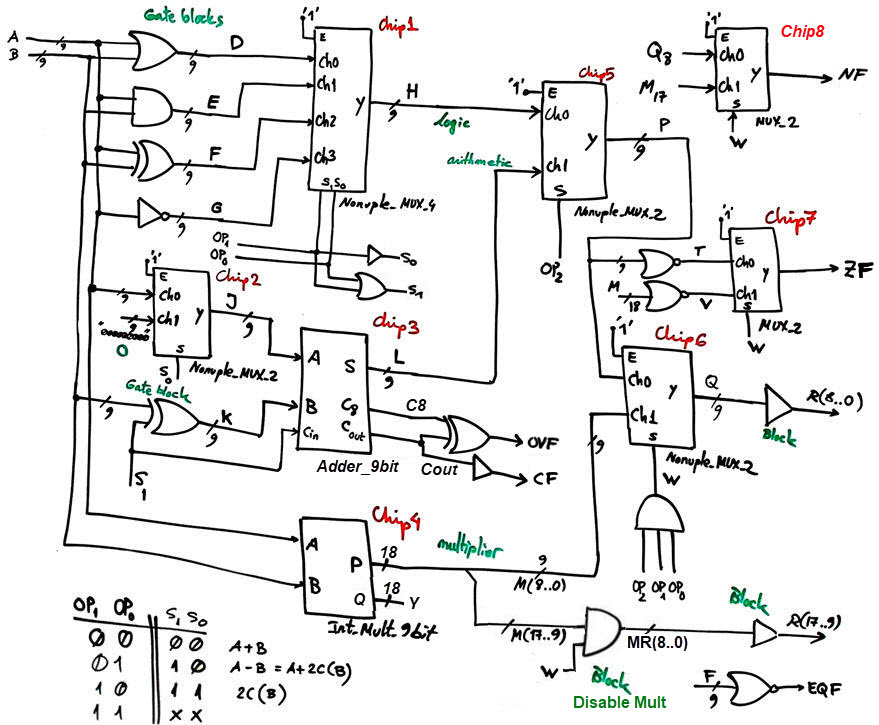 |
|
Fig. 3a. Proposed ALU internal design. |
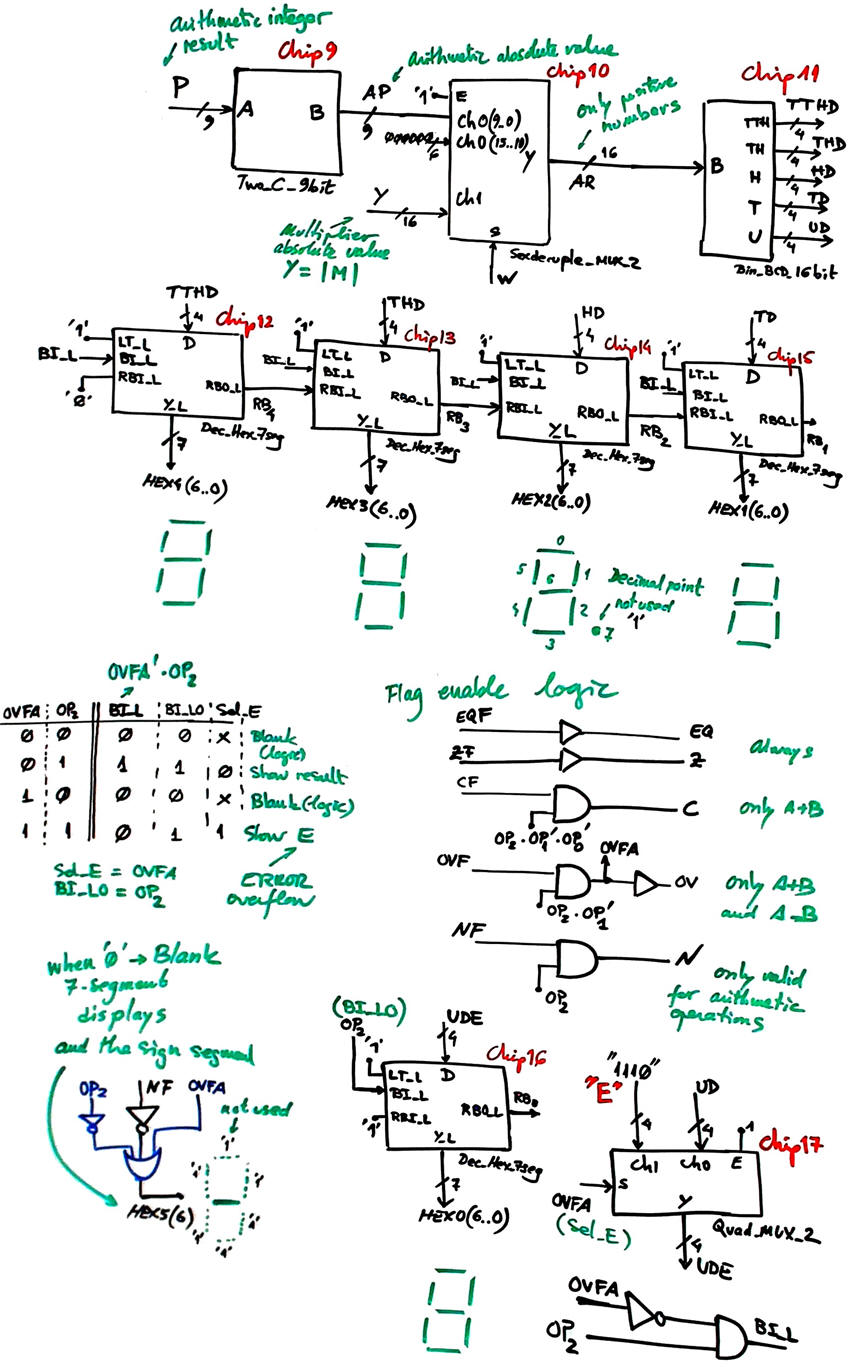 |
|
Fig. 3b. Additional circuits for using the 7-segment displays and for enabling the flags. |
The Chip9 Bin_BCD_16bit converter for representing results in BCD will be connected to the signal Y(15..0) when performing multiplications (OP = 7), or to the signal L(8..0) when OP = 4, 5, 6. The display will be kept blank for logic bitwire operations (OP = 0, 1, 2, 3).
Thus, the full list of FPGA input and output connections is represented in Fig. 4.
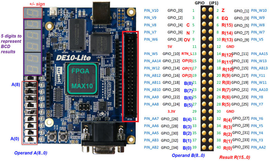 |
|
Fig. 4. FPGA connections to be used in the pin assignment tool. Board LED and other unused segments will be blanked. |
3. Development
FPGA circuit. We can translate into VHDL the top schematic ALU_9bit.vhd in Fig. 3a and Fig. 3b, synthesise and test the FPGA using Quartus Prime and ModelSim respectively.
These are the multiplexers used to select operands and operations: Nonuple_MUX_4.vhd, Nonuple_MUX_2.vhd, MUX_2.vhd , Quad_MUX_2.vhd, Sexdecuple_MUX_2.vhd. All of them are implemented in a single file adapting the typical plan B Dual_MUX_4.
Annex A1 shows how to design a carry-lookahead (CLA) version of the Adder_9bit.
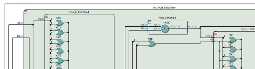
Int_Mult_9bit tutorial shows how to implement a 9-bit multiplier for interger numbers as required in Chip4.
 |
|
Fig. 5. Detail on the Int_Mult_9bit RTL. |
Bin_BCD_16bit shows how to design the converter from radix-2 to BCD for a size of 16-bit. You will find its top entity and its component block DM74185.
Chip9 on implementing a two's complement Two_C_9bit can be found in Int_Mult_9bit tutorial.
We can continue adding the code converters to represent the result in the six 7-segment displays. The idea is that the sign is represented as a hyphen '-' when the result is negative in the display number 5 (HEX5_L(6)). This is the decoder hexadecimal to 7-segments Dec_Hex_7seg and its block Hex_7seg_decoder that can be either plan A or plan B.
All the VHDL files required in this hierarchical modular prototype: ALU_9bit.zip.
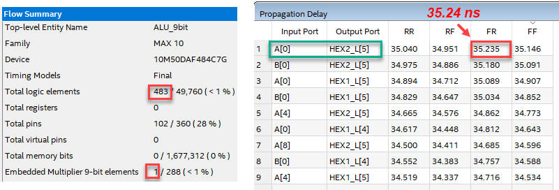
We observe how the project summary shows the use of a dedicated multiplier (one of the 288 available). This is given you an initial idea of the size and complexity of the circuits that can be engineered to fit in this target chip.
 |
|
Fig. 6. Project summary and propagation delay. |
The circuit uses 483 logic elements and 1 embedded multiplier. Switching A(0) and waiting for the HEX2_L(5) output function takes the longest signal path, a worst case scenario propagation delay of tP = 35.24 ns. If we attach A(0) to a signal generator the maximum signal frequency is fmax < 14.18 MHz).
PCB. As indicated above, in this experiment we can use the board's switches to input A(8..0). The other operant B(8..0), the operation selector OP(2..0) and the 5 status flags (N, OV, C, Z, EQ) will be placed in an auxiliary PCB connected through the 40-pin GPIO as shwon in Fig.4.
We have to capture the schematic in KiCad schematic as shwon in Fig. 7. LED bars and resistors packs can be used to save board space.
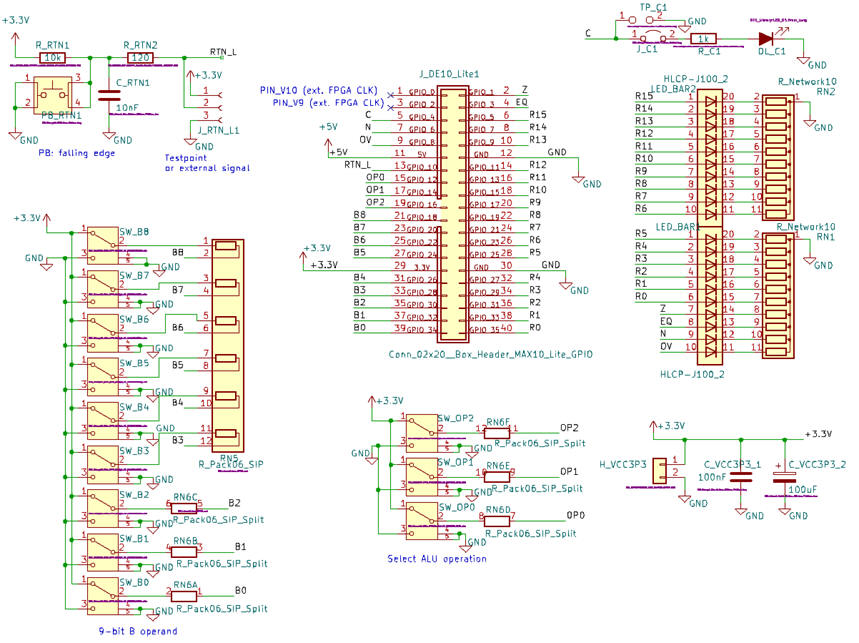 |
|
Fig. 7. Schematic captured in KiCad. |
The PCB component placement is shown in Fig 8.
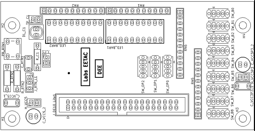 |
|
Fig. 8. PCB layout silkscreen that shows component placement and references. |
Finally, a 3D view shows the real dimensions and how the PCB will look like once soldered.
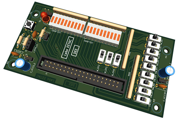 |
|
Fig. 9. PCB 3D representation. |
Thus, once the hardware circuit for the PCB is conceived, we organise a KiCad project CSD_LAB4_PCB_v1.zip. Each component contains the symbol, the footprint, and a link to the datasheet to prepare the bill of materials (BOM) spreadsheet. Current CSD and DEE KiCad symbols, footprints and 3D tuned components are available in these three libraries 3dmodels.zip, footprints.zip, symbols.zip, to be unzipped for instance in the user directory.
4. Test
It is convenient to perform a functional simulation to check that the circuit operates correctly before configuring the target chip with the programmer application. This is a testbench ALU_9bit_tb.vhd adapted from P4. This is the wave setup as shwon in Fig. 10. wave.do.
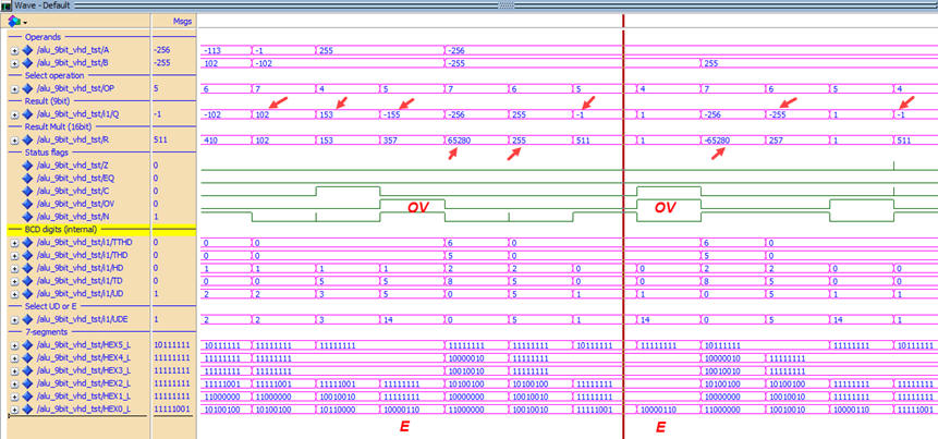 |
| Fig. 10. ModelSim simulations. Be aware that for arithmetic operations 4, 5, and 6, the result of interest is Q(8..0) or R(8..0). |
The pin assignment file to be imported to the project is ALU_9bit_prj.csv.
This is the final FPGA ALU_9bit.sof configuration file to be used by the Quartus Prime programmer.
The final board prototype is pictured in Fig. 11. This is the full KiCad project zip file and the KiCad libraries containing adapted symbols and footprints.
 |
|
Fig. 11. Prototype connecting the inputs and outputs board to the DE10-Lite training board. |
Laboratory measurements using the compact VB8012 instrument driving the 3-bit signal OP. Check whether speed measurements can be visualised. Compare your lab results with measurements from Quartus Prime timing analyser.
|
|
|
Fig. 12. Measurements when the ALU_9bit is operating. |
Annexes
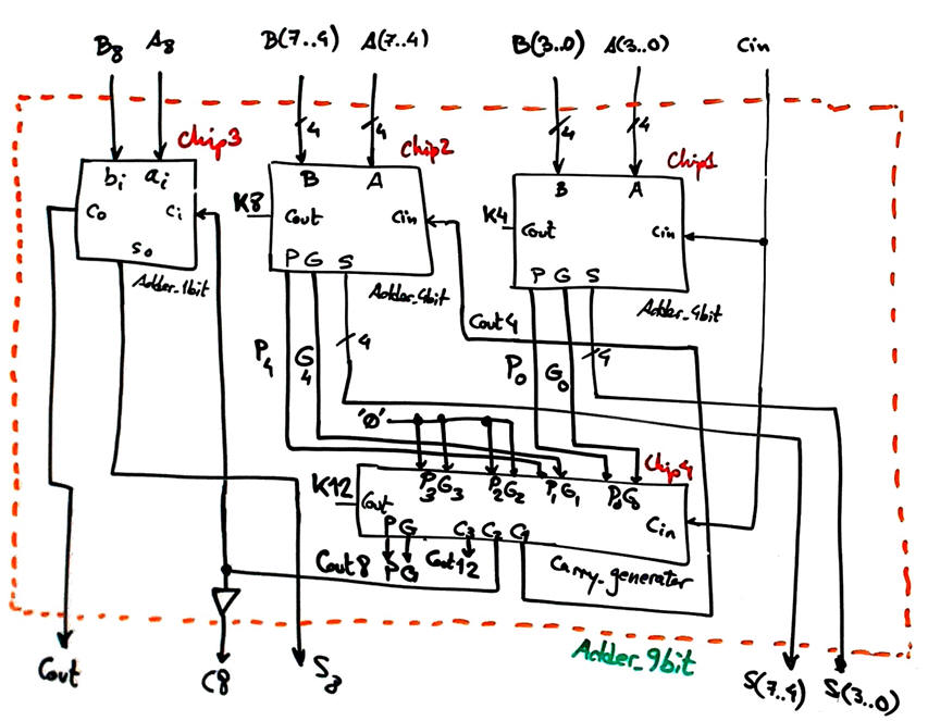
A1. Example of planning the Adder_9bit using CLA option from the tutorial Adder_16bit above.
|
|
|
Fig. 1. Adder_9bit symbol and truth table. |
We can invent it as the other similar circuits, using plan C2.
 |
|
Fig. 2. Proposed Adder_9bit. |
This is the VHDL translation of the Fig. 2 scheamtic: Adder_9bit.vhd , Adder_4bit (it includes the Adder_4bit and the Carry_Generator), Adder_1bit (for example plan A)
| Home Term 23/24-Q2 Contact Products Electronic devices and companies Software Books Magazines Instruments DEE Library EETAC DEEL |

|
|
| Web activa des de 09/2001, @ F. J. Robert, J. Jordana. Web editat amb Microsoft Expression Web 4. El contingut és un complement als materials d'estudi del curs Circuits i Sistemes Digitals disponibles al campus digital Atenea. Llicència:Reconeixement 4.0 Internacional de Creative Commons |