|
|
Bachelor's Degree in Telecommunications Systems and in Network Engineering |
|
|
|
Using and designing data-type flip flop (D_FF) |
1. Specifications (using the chip)
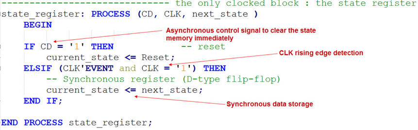
The D_FF device is the preferred memory cell to build the state register of a FSM. Let us see how to write it in VHDL using behavioural style. This is the complete design process rec.
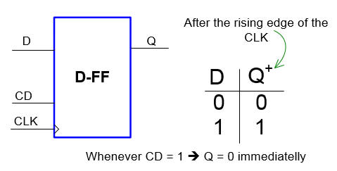 |
Fig. 1a). Typical symbol and function table including CLK and clear direct CD asynchronous reset.
Commercial synchronous 1-bit D_FF memory cell type 74HCT74 or 74LS273. |
 |
|
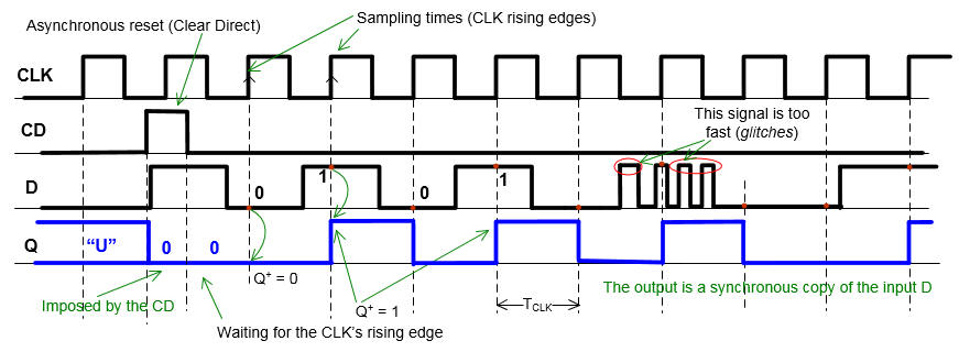
| Fig. 1b) Example timing diagram of a data flip-flop D_FF. Clear direct (CD) and set direct (SD) are respectively the asynchronous reset and set. (Visio). |
|
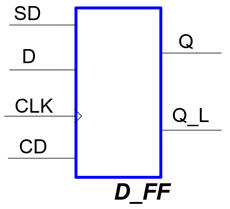 |
Fig. 1c) Complete symbol including asynchronous set (SD) and also the complemented output Q_L. |
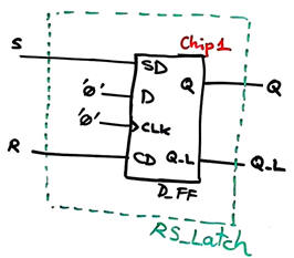 |
Fig. 1d) If the synchronous input D is not used (CLK = D = '0'), the D_FF becomes an asynchronous RS_Latch. |
2. Planning for designing the chip
In Fig. 2 there is the circuit's state diagram. It is the best tool to describe how it works complementing the function table. State transitions (arrows) are only possible when there is a CLK's rising edge (the idea of CLK synchronicity). And because it happens for all the transitions we have decided not to annotate it to make a clearer representation. Thus, remember that when you see for example D = 1, it means D = 1 and CLK rising edge.
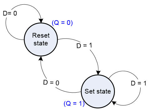 |
Fig. 2. State diagram where the arrows indicate the transitions between states accordingly to the given condition, and, in parenthesis in each state there is the indication of the output values. To make it easy, different colours are used to represent outputs and transitions. |
Version 1 for writing the D_FF into VHDL (as in many books)
This device is easily written in VHDL as seen in Fig. 3 as a behavioural description (plan B). This D_FF component is to be found anywhere. For instance, as the process for implementing the state register of a FSM.
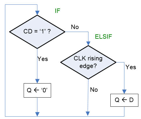 |
Fig. 3. The flow chart that solves the functionality of the D_FF. |
Version 2 for writing the D_FF into VHDL (as in CSD FSM style)
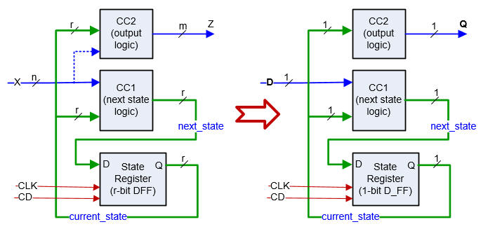
Another way to plan the D_FF, which is translating the state diagram into an architecture, is to conceive it as a FSM, in the same way that here in CSD the other JK_FF and T_FF have been organised. Fig 4 shows the general FSM architecture adapted to the D_FF.
 |
|
Fig. 4. The FSM conception and the adaptation to a D_FF component (vsd). |
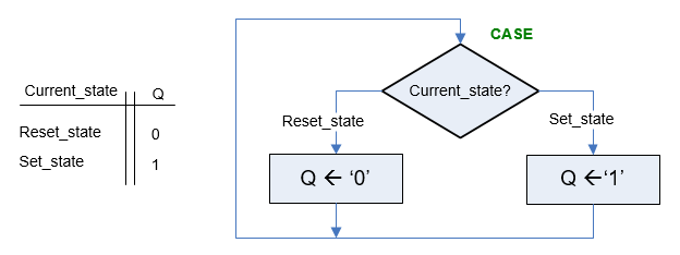
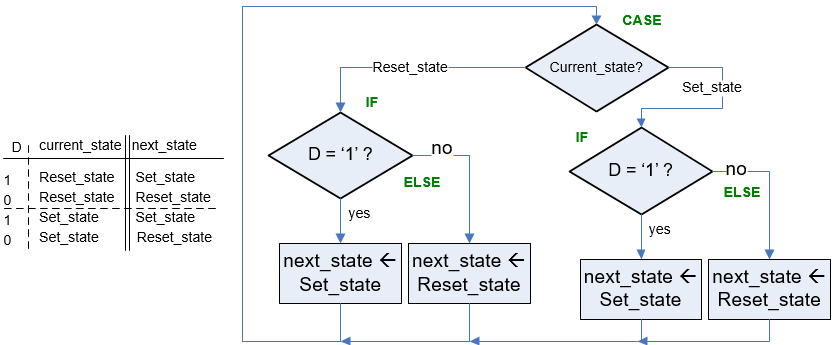
Therefore now, the only thing left is the CC1 and CC2 truth tables and their corresponding behavioural interpretations as flowcharts ans shown in Fig. 5.
 |
 |
|
Fig. 5. The CC1 and CC2 trutht tables and flowcharts derived from the state diagram. |
3. Development
This is the version 1 of the D_FF.vhd as a simple process (the way it is used in the FSM's state register) and the exact translation of the flow chart in the Fig.3 above.
This is the version 2 of the same D_FF.vhd translating the the FSM style in Fig. 4, as it is used all the time in our CSD course. Naturally, for this simple D_FF, after synthesising the VHDL project, the CC1 and CC2 are reduced to a simple buffer or wire because the state register is already a D_FF:
NOTE: This is the complete D_FF with both, CD and SD asynchronous inputs (Fig. 1c): D_FF.vhd. In this way, if desired, this chip can be used as a component to implement an RS_Latch (Fig. 1d).
Whatever the styles, the synthesiser interprets correctly both behavioural descriptions producing the RTL picture in Fig. 6.
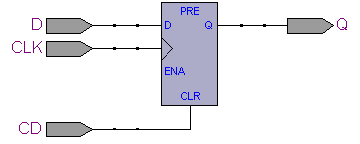 |
Fig. 6. The RTL symbol for the D_FF. Generally, we'll use the CD (CLR)asynchronous signal to reset the memory cell when starting operations or in the case where is required to go back to a know state. The SD (PRE) set direct is not used in this model. |
And thus, the key point here is that the synthesiser interprets correctly that you have in mind a 1-bit memory cell that corrently is also called register, as shown in the summary report in Fig.7.
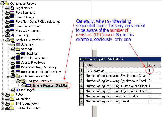 |
Fig. 7. Number of registers used in the synthesis of the circuit. |
4. Testing (functional)
This in Fig. 8 is the VHDL testbench schematic that we have in mind to run simulations. To test CLK-driven sequential systems at least two concurrent stimulus processes will be required: one process for the CLK and another one for all the other input signals.
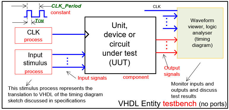 |
| Fig. 8. Testbench where to make it easy the CLK is another concurrent process. (visio) |
For testing the circuit D_FF the general testbench schematic in Fig. 8 is adapted as shown in Fig. 9.
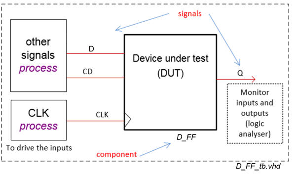 |
Fig. 9. VHDL testbench. Let us use two processes to drive the inputs and the CLK. Or instead, you can use three processes working concurrently, one process for ech type of input. |
Start the test bench template and add the CLK and inputs activity translating the timing diagram in Fig.1. Make all the timing relative to the CLK_Period constant, which is the equivalent in Chapter 2 to the Chapter 1 constant Min_Pulse.
This is a sample test bench file D_FF_tb.vhd. It contains a glitch, the meaning of which is a fast signal (shorter than one CLK period) that is not detected by the system. Thus, for a given system, the CLK has to be faster than any input to be processed because if not, it is not seen.
Run the EDA VHDL tool and demonstrate how the circuit works adding comments to the printed sheet of paper containing the waveforms.
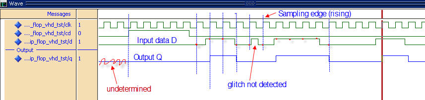 |
| Fig. 10. Example of a timing diagram to show how the circuit works. |
NOTE: This is an example testbench D_FF_tb.vhd, wave.do, driving SD, CD, CLK and D for the D_FF complete symbol drawn in Fig. 1c.
5. Testing (gate-level and timing analiser)
Gate-level simulation and timing anayser. Which is the maximum circuit's speed? For instance Fig. 11 shows the propagation time from CLK to output delay measurement in a MAX II EPM2210F324C3.
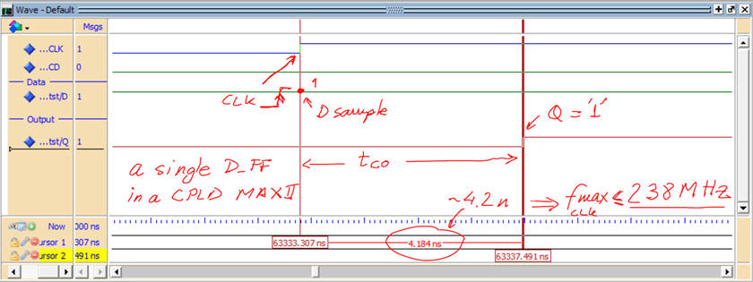 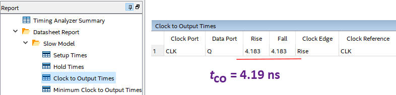 |
| Fig. 11. Example of measurements in a transition from CLK to output. |
6. Report
Project report starting with the template sheets of paper, scanned figures, file listings, docx , pptx, or any other resources
7. Prototyping
Use training boards and perform laboratory measurements to verify how the circuit works.
| Home Term 24/25-Q1 Contact Products Electronic devices and companies Software Books Magazines Instruments DEE Library EETAC DEEL |

|
|
| Web activa des de 09/2001, @ F. J. Robert, J. Jordana. Web editat amb Microsoft Expression Web 4. El contingut és un complement als materials d'estudi del curs Circuits i Sistemes Digitals disponibles al campus digital Atenea. Llicència:Reconeixement 4.0 Internacional de Creative Commons |