|
|
||
|
|
MDS: Multiplexed display system for 7-segment digits |
|
|
|
||
1. Specifications
When using the prototyping board Nexys 2 from Digilent, we need to invent a driver for the four 7-segment digits. Fig. 1 shows how the displays are interfaced with the FPGA, where only 12 pins are used. We can name it scanning display controller circuit in a similar way we did with the 16-key matrix encoder, or for instance multiplexed display system (MDS).
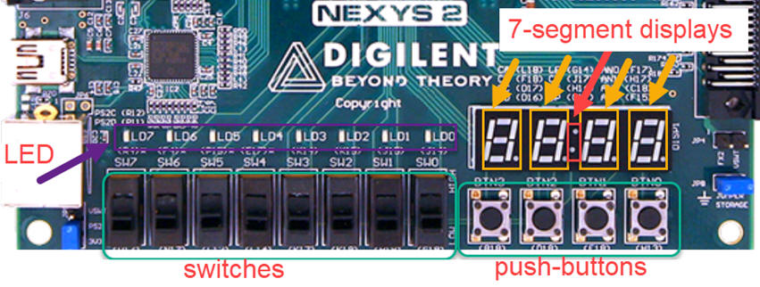 |
| Fig 1. Picture of the Nexys 2 board indicating the input and output resources, one of which are the four multiplexed displays. |
Applications such calculators may used this MDS technique for visualising up to 12 digits with a low pin count (only 19 instead of 84)
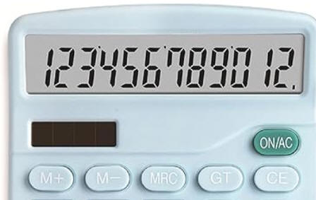 |
| Fig 2. Calculator display where up to 12 digits may be driven by a multiplexed display controller. |
From the datasheet we can see the connections details, as represented in Fig. 3. The four 7-segment displays, common anode, are sharing the same cathode connections and the digit anodes are activated by PNP transistors. The idea is to multiplex in time at high speed, for instance 1 kHz, so that only one of the four digits is active and our eyes integrate light so that all the four digitls appears equally illuminated, as in many other display and screen devices.
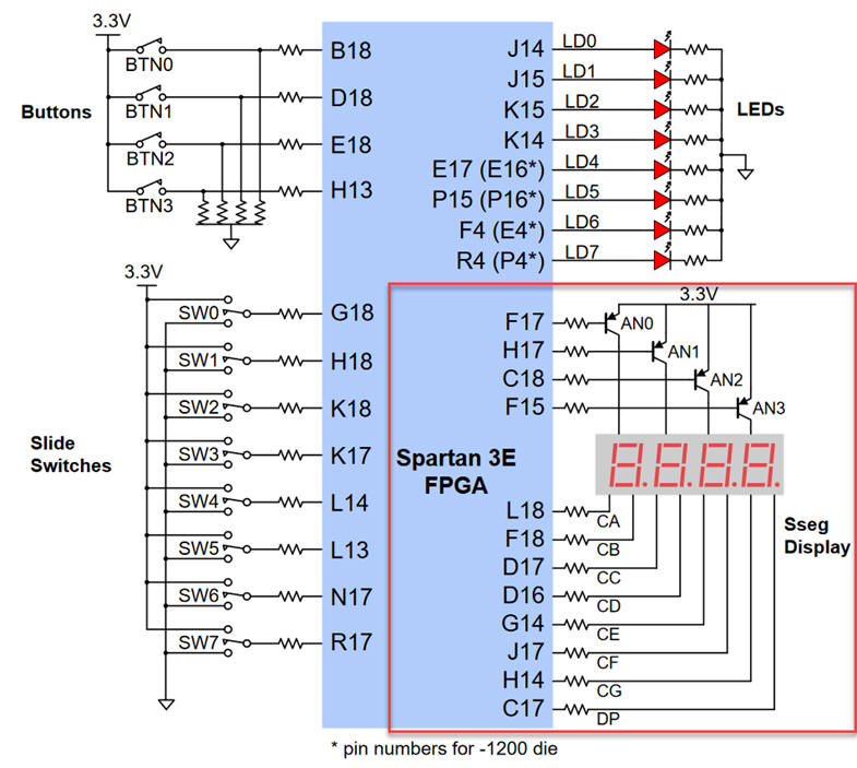  |
| Fig. 3. Connecting input and outputs resources to FPGA pins. All the four digits available share the same A, B, C, D, E, F, G segments cathodes. |
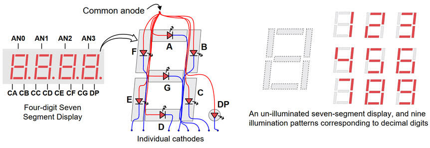
Fig. 4 shows from the datasheet the idea of multiplexing display symbols accordingly to the activation of the corresponding anode. This is the task to be performed by the MDS symbolised in Fig. 5.
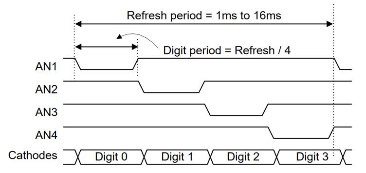 |
| Fig 4. Connecting input and outputs resources to FPGA pins. |
Entity symbol and input and output connections.
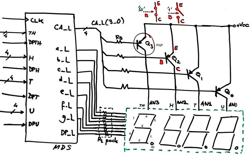 |
| Fig 5. Proposed symbol of the MDS and how it is connected in the NEXYS 2 board. |
2. Planning
Let us use plan C2. Inventing the MDS requires using several standard combinational and sequential components and as usual many options are possible. For instance:
- Option #1: Counting in binary radix-2 and decoding using a Dec_2_4 to obtain the one-hot sequency to drive the anodes.
- Option #2: Counting directly in one-hot.
Additionally we can conceive the counter modulo 4 using the versatile Counter_mod16 for both:
- Option #3: truncating at '0011'
- Option #4: Implementing the necessary load signals to jump for counting directly in one-hot
The counter modulo 4 can also be implemented using other standard sequential blocks such:
- Option #5: 4-bit data register
- Option #6: 4-bit shift register
In this tutorial we show you option #1 realisation as represented in Fig. 6.
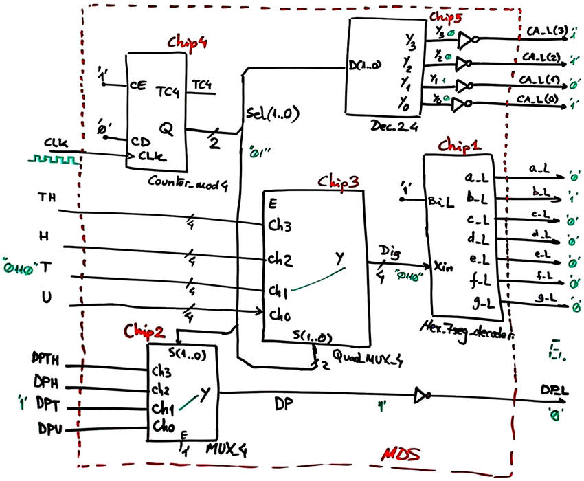 |
| Fig 6. Proposed architecture for the MDS. |
The functionality of the MDS circuit can be observed in an application such the highlighted Timer_MMSS prototype, where is replacing the four Hex_7seg_decoder.
Project location:
C:\CSD\P7\MDS\(files)
3. Development
MDS.vhd is the translation into VHDL of the schematic in Fig. 6. Its internal components can be collected and adapted from the products page: MUX_4.vhd, Quad_MUX_4.vhd, HEX_7SEG_DECODER.vhd, Dec_2_4.vhd and Counter_mod4.vhd.
4. Test (functional)
 |
| Fig 7. Testbench fixture to check how the MDS works. |
 |
| Fig 7. VHDL simulation to show how the circuit works accordingly to the timing diagram in Fig. 4. |
5. Prototype using NEXSYS 2 board
For testing this subsystem, as we did in the simulation, we can imagine fixed values for TH, H, T and U digits. Additionally, in the prototype, we can add a switch to select two scanning speeds: 2 Hz and 200 Hz, which are generated by a CLK_Generator circuit.
 |
| Fig 8. Planning the prototype. |
 |
| Fig 9. Circuit running. |


