|
|
Bachelor's Degree in Telecommunications Systems and in Network Engineering |
|
|
|
|||||
Chapter 3 problems |
- B3.13 - |
Encoder 12-to-4, Encoder 3-to-8 (μC - C) |
|||
|
|
|||||
1. Specifications
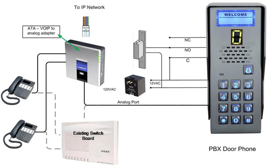
The project objective is to design an encoder Enc_12_4 similar to the one presented in tutorial Enc_10_4 using a µC. For instance, the application can be integrated as a subsystem in a professional PBX door phone with dialing keypad as represented in Fig. 1. The device has to generate the 4-bit code of the clicked key. BCD codes for keys from 0 to 9, "1010" for the hash symbol "#" and "1011" symbol for the asterisk symbol "*". Group select output (GS) has to be held high when any key is pressed. The encoder also has enable input (Ei) and enable output Eo to detect when it is disabled and when is active but no one is pressing keys. Finally, a 7-segment output will represent the code of the key pressed.
The same project is proposed in D1.13 as a combinational circuit based on logic gates.
 |
|
Fig. 1. The keyboard that that has to be interfaced to a commercial PBX and the commercial reference of the diagram |
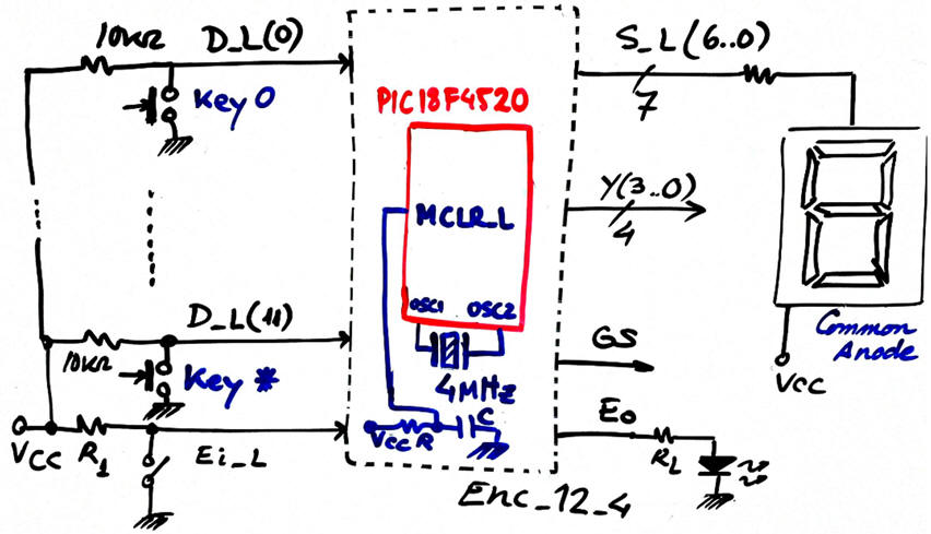
The emphasis is set therefore in learning basic polling digital inputs and writing digital outputs. The truth table will be solved using a behavioural plan B interpretation in C language, organising the hardware-software diagram so that the input and outputs variables will be saved in RAM memory. Your planning has to be similar to the one discussed in Chapter 1 D1.13, but using C code instead of VHDL. The symbol for the Enc_12_4 that will have priority high as usual in this kind of devices is represented in Fig. 2.
 |
|
Fig. 2. Enc_12_4 symbol and the idea of designing it using a µC. |
Some questions and ideas to organise the project:
Draw the truth table for the Enc_12_4. Draw an example timing diagram.
You can solve the circuit in several steps, adding a few lines of code each time to develop and test immediately. And also the features can be added in phases:
- step #1 only the basic encoding function and the output Y
- step #2: GS, Ei, Eo
- step #3: add the 7-segment outputs S_L.
A) Planning hardware
Copy and adapt a circuit from any of the previous projects (LAB9) and name it Enc_12_4.pdsprj. Assign pins to inputs and outputs accordingly to one of the following options (your instructior will tell you which):
Pin assignment option #1:
D_L(7..0) --> RB(7..0); D_L(11..8) ---> RC(3..0)
Ei_L --> RA4; Eo --> RA3; GS --> RA2;
S_L(7..0) --> RD(7..0)
Y(3..0) --> RC(7..4)
Pin assignment option #2:
D_L(7..0) --> RD(7..0); D_L(11..8) ---> RC(7..4)
Ei_L --> RA2; Eo --> RA4; GS --> RA3;
S_L(7..0) --> RB(7..0)
Y(3..0) --> RC(3..0)
Pin assignment option #3:
D_L(7..0) --> RB(7..0); D_L(11..8) ---> RD(7..4)
Ei_L --> RA1; Eo --> RA3; GS --> RA2;
S_L(7..0) --> RC(7..0)
Y(3..0) --> RD(3..0)
Project location:
C:\CSD\P9\Enc_12_4\(files)
B) Planning software
Organise the main program in our CSD way.
Propose a hardware-software diagram naming all the electrical signals, RAM variables and the software functions.
Describe all the RAM memory variables used in this project and its type. How many bytes does var_D occupy?
Explain how to configure the µC in init_system(). List all RAM variables required and their type.
Organise using a flowchart the interface function read_inputs().
Organise using a flowchart the interface function write_outputs().
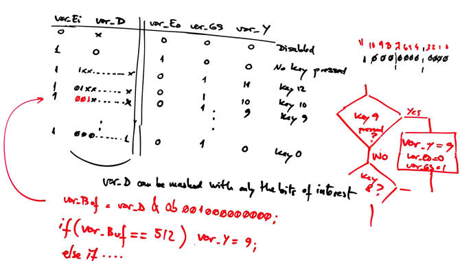
Infer the truth_table() software function using a behavioural interpretation and the corresponding flowchart. Fig. 3 shows an initial sketch after having read the Chapter 1 Enc_10_4 tutorial circuit. Probably both, switch-case or if-elseif statatements can be used in this translation.
 |
|
Fig. 3. Enc_12_4 initial discussion on adapting the truth table using plan B flowcharts. |
Developing & testing (debugging)
Write the Enc_12_4.c source code translating the function flowcharts. Start capturing only one input as in (LAB9) and visualising it in the watch window. And only then go step by step developing & testing more inputs.
Start a software IDE project for the target microcontroller PIC18F4520 and generate the configuration files ".cof" and ".hex" after compilation. Discuss the project summary: % of ROM used for the code, number of RAM bytes used, etc.
| Note: Step-by-step tactical approach for developing and testing the project: Read one input at a time and run to check that the voltage value is correctly captured as a valid digital value in RAM memory. Write one output at a time and run to check that your code is correct to light the LED connected at the output pin. |
Add a few lines of code every time, compile and run the test intereactively to check results watching variables.
Measure how long does it take to run the main loop code when using a 4 MHz and a 16 MHz quartz crystall oscillator.
| Home Term 23/24-Q2 Contact Products Electronic devices and companies Software Books Magazines Instruments DEE Library EETAC DEEL |

|
|
| Web activa des de 09/2001, @ F. J. Robert, J. Jordana. Web editat amb Microsoft Expression Web 4. El contingut és un complement als materials d'estudi del curs Circuits i Sistemes Digitals disponibles al campus digital Atenea. Llicència:Reconeixement 4.0 Internacional de Creative Commons |