|
|
Bachelor's Degree in Telecommunications Systems and in Network Engineering |
|
|
|
|||||
Chapter 1 problems |
- D1.13 - |
Encoder 12-to-4, Encoder 3-to-8 |
|||
|
|
|||||
Modif
option #1:
1. Specifications
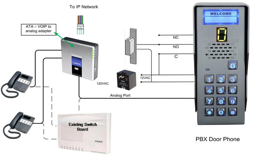
The project objective is to design an encoder Enc_12_4 similar to the one presented in the tutorial Enc_10_4 using VHDL synthesis and verification tools. For instance, the application can be integrated as a subsystem in a professional PBX door phone with dialing keypad as represented in Fig. 1. The device has to generate the 4-bit binary code of the clicked key. BCD codes for keys from 0 to 9, "1010" for the hash symbol "#" and "1011" symbol for the asterisk symbol "*". Group select output (GS) has to be held high while any key is pressed. The encoder also has enable input (Ei) and enable output Eo to detect when it is disabled and when is active but no one is pressing keys. Use a 7-segment decoder from any of the tutorials to represent the code of the key pressed.
The same project B3.13 is proposed in Chapter 3 for learning the basics of μC software organisation and basic digital I/O.
 |
|
Fig. 1. The keyboard that that has to be interfaced to a commercial PBX and the commercial reference of the diagram |
Propose the symbol and truth table of this Enc_12_4 adapting other encoder examples.
Draw an example of timing diagram to be used later as stimulus in the testbench when verifying the synthesised circuit. Consider Min_Pulse = 2.67 ms.
As a good design strategy, you can organise the project in two design phases:
- phase #1: You can imagine a symbol and a circuit similar to the Enc_10_4 and so not including yet the outputs a, b, c, d, e, f, and g to be able to connect a 7-segment display. Develop and test this project. When this circuit with only binary radix-2 outputs Y(3..0) works correctly, and only if you have more time,
- phase #2: Add the new segment outputs to the phase #1 truth table so that you can also light a 7-segment display as shown in Fig.1.
CPLD or FPGA target chip options:
Target chip #1.: MAX II
Target chip #2.: MAX 10
Target chip #3.: Cyclone IV
2. Planning
Plan A: Find equations and write them in a single VHDL file. For example:
option #1: PoS from minilog minimisation software or by inspection of the truth table. Write down the single-file (flat) VHDL code using equations. Synthesise and test.
Project location:
C:\CSD\P2\Enc_12_4\planA1\(files)
option #2: SoP from minilog minimisation software or by inspection of the truth table. Write down the single-file (flat) VHDL code using equations. Synthesise and test.
Project location:
C:\CSD\P2\Enc_12_4\planA2\(files)
Plan B: capture in a single VHDL file the truth table drawing firstly an schematic. Synthesise and test.
Project location:
C:\CSD\P2\Enc_12_4\planB\(files)
Plan C2: draw a hierarchical circuit using Enc_4_2 components and logic gates if necessary. Synthesise and test.
Project location:
C:\CSD\P2\Enc_12_4\planC2\(files)
option #2: Binary encoder 8-to-3, type 74LS148
1. Specifications
Fig. 1 shows the block diagram and the truth table of an 8-to-3 encoder (Enc_8_3), a typical P2 example of standard circuit. When several inputs are active high at the same time, a binary code is generated of the highest priority signal. The symbol "-" means a "don't care" value that is represented other times by "x". GS goes high when any input is assessed, thus it can be used both as a flag to indicate that a key is pressed and for disambiguation of the code "000".
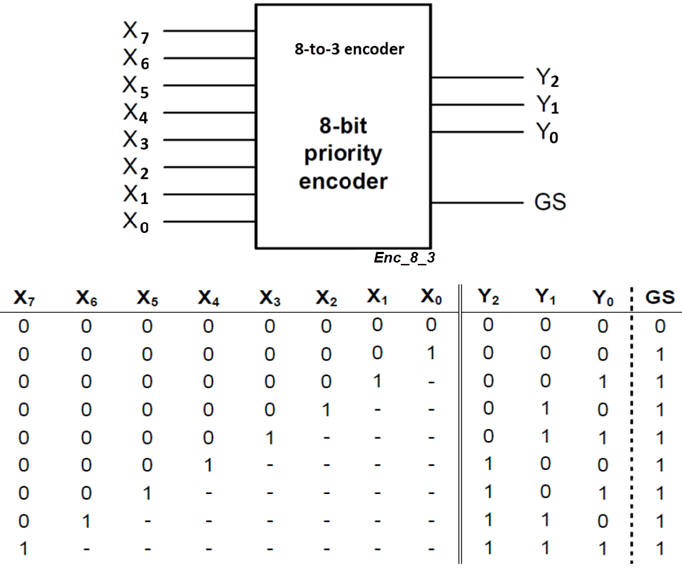 |
|
Fig. 1. The symbol and truth table of a combinational circuit. |
Study if it is possible to obtain easily the canonical functions for the four circuit outputs.
Represent the output GS using maxterms. How many minterms will the function have?
2. Planning
Plan A
Find PoS or SoP using Minilog minimisation software or by inspection of the truth table.
Write down the single-file (flat) VHDL code using equations.
Plan B
Capture in a single VHDL file the truth table drawing firstly an schematic.
Plan C2
Draw a hiearchical circuit using Enc_4_2 components and logic gates if necessary.
| Home Term 23/24-Q2 Contact Products Electronic devices and companies Software Books Magazines Instruments DEE Library EETAC DEEL |

|
|
| Web activa des de 09/2001, @ F. J. Robert, J. Jordana. Web editat amb Microsoft Expression Web 4. El contingut és un complement als materials d'estudi del curs Circuits i Sistemes Digitals disponibles al campus digital Atenea. Llicència:Reconeixement 4.0 Internacional de Creative Commons |