|
|
Bachelor's Degree in Telecommunications Systems and in Network Engineering |
|
|
|
|||||
Chapter 1 problems |
- D1.14 - |
9-bit parity generator, parity checker |
|||
|
|
|||||
1. Specifications
The project objective is to design a 8-bit data transmitter and receiver system with parity bit generator and checker. Fig. 1 shows the idea. The circuit relies on the component Parity_9bit type 74LS280. Transmission channel induced errors of 1-bit switch can be simulated using a XOR gate. If the data received is wrong and error flag is generated and the received byte is reset. Implement the system in VHDL using plan C2.
The same project B3.14 is proposed in Chapter 3 for learning the basics of μC software organisation and basic digital I/O.
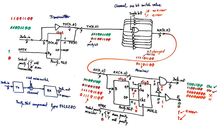 |
| Fig. 1. 8-bit parallel transmission system with addition parity bit. |
Draw an example of timing diagram to be used later as stimulus in the VHDL testbench when verifying the synthesised circuit. Consider Min_Pulse = 3.78 ms.
CPLD or FPGA target chip options:
Target option #1.: MAX II
Target option #2.: MAX 10
Target option #3.: Cyclone IV
This transmission system can be serialised in P7 and P8 using shift registers, as shown in the tutorial USART.
| Home Term 23/24-Q2 Contact Products Electronic devices and companies Software Books Magazines Instruments DEE Library EETAC DEEL |

|
|
| Web activa des de 09/2001, @ F. J. Robert, J. Jordana. Web editat amb Microsoft Expression Web 4. El contingut és un complement als materials d'estudi del curs Circuits i Sistemes Digitals disponibles al campus digital Atenea. Llicència:Reconeixement 4.0 Internacional de Creative Commons |