|
|
Bachelor's Degree in Telecommunications Systems and in Network Engineering. Bachelor's Degree in Aerospace Systems Engineering |
|
|
|
|
|
|
Project: hobbyist climate chamber |
|
|
|
Project specifications |
Our goal is to design a control system for a hobbyist climate chamber intended for temperature test.
Chamber constant temperature at the reference point above ambient temperature can be attained using simple heating elements (power resistors); using a thermoelectric cooler (TEC) cell we can obtain chamber temperatures below room temperature. Local temperatures below 0 °C over small surfaces, for example for cooling electronic chips, are also possible using multi-stage TEC devices.
|
|
|
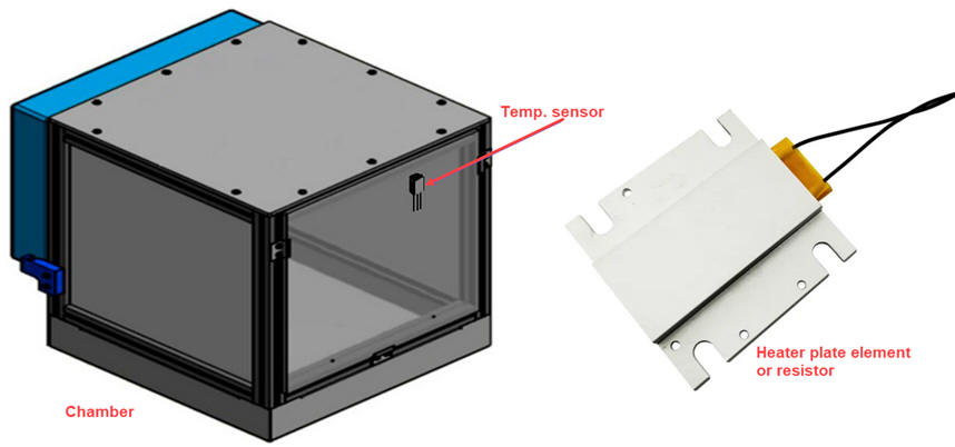
Fig. 1. Small climate chamber for hobbyist (picture ref.) |
With the aim of designing several introductory circuits, let us consider a room temperature range from 15 °C (outdoor winter or air conditioned room) to 27 °C. A sensor type LM35 will be glued insider the chamber to measure the current temperature TS (°C) and a potentiometer with an LCD readout will supply the reference temperature TR (°C).
We will invent the control circuit as an opportunity for reusing and chaining previous content and projects. Let us imagine several design phases as if the circuit has to evolve adding new features and modules. For instance:
- Design phase A: Analogue system
0.- Heating and cooling elements: resistors and thermoelectric cells.
1.- Simple comparator-based analogue control.
2.- Hysteresis window.
3.- Linear control. Plant modelling. PID equation.
- Design phase B: Digital
0.- Temperature monitor LCD for measuring TS (°C) and TR (°C). Introduction to Arduino.
1.- Digital ON/OFF control comparing TS (°C) and TR (°C). PWM signals for power regulaton.
2.- Hysteresis-based PWM control.
3.- Digital control loop.
- Design phase C. Power supply
1.- Linear power supply for the electronic circuit and heating/cooling actuators
2.- Switching mode power supply
3.- Batteries, solar cells, etc.
- Design phase D. Communication interfaces
1.- Serial
2.- Bluetooth
3.- Wi-Fi, etc.
In phases A and B laboratory power supplies will be used as energy sources for driving circuits and heating elements (actuators).
References and additional questions
A good reference on what we are indenting to discuss in this introductory project can be read in this paper.
Study how to control as well the chamber's relative humidity.
|
|
||
|
|
Design phase A0: heating and cooling elements |
|
|
|
||
A0 specifications |
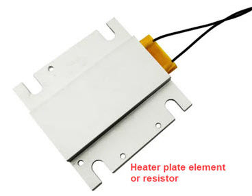
Heating element (power resistor)
Joule heating is the process by which the passage of an electric current through a conductor produces heat. This heat will be dissipated warming the surrounding air above ambient temperature.
|
|
Fig. 2. Air heater plate commercial element. |
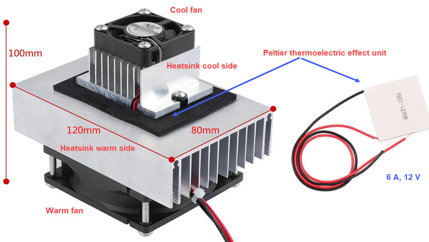
Peltier heating/cooling cell
Thermoelectric cells generate heat and cool depending on electrical current direction through the element. They are based on Peltier effect.
Chamber constant temperature at the reference point below ambient temperature will be attained using a thermoelectric cooler (TEC) cell type TEC1-12706.
|
|
|
Fig. 3. Thermoelectric cell kit including mounted hot and cold heatsinks and fans. TEC elements have a wide range of industrial applications, for example, for stabilising the temperate of power laser diodes using sophisticated full bridge bidirectional PWM controllers. This is another interesting reference on how TEC cells are used for cooling objects. |
|
|
||
|
|
Design phase A1: analogue control system |
|
|
|
||
1. A1 specifications |
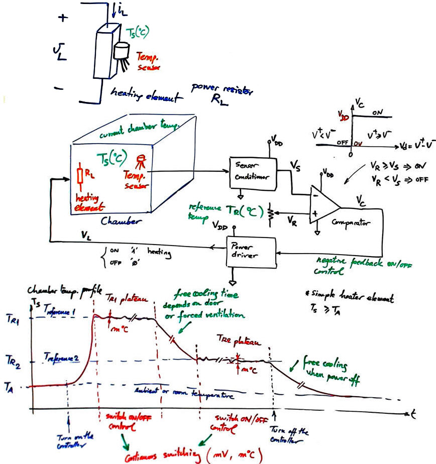
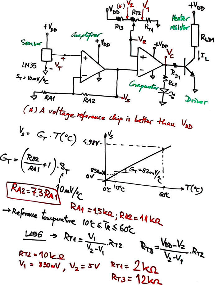
The chamber contains a simple heating element, a power resistor for instance, as showm in Fig. 1. The initial idea for an electronic control systems is to maintain the surface of the heating element to a given reference temerature value.
|
|
|
Fig. 1. Basic idea, control system using an analogue comparator. This ON/OFF feedback control loop tracks TR with precision due to the high gain of the comparator amplifier. A few m°C of difference between the current temperature in the chamber and the reference generates a differential voltage of a few mV enough to switch the comparator output, and, as a consequence, the heater element is switching continuously. |
2. Planning
Hardware
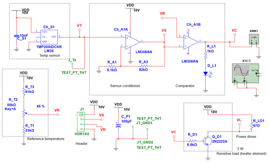
The proposed block diagram is shown in Fig. 1. It is based on using an OpAmp as comparator. The initial idea is keep the heating element (power resistor) working above room temperature from 30°C to 60 °C and implement a first experiment on controlling temperature at a given reference point.
As an starting point for this phase A design, we can imagine only positive temperatures from 10 °C up to 60 °C (indeed, above room temperature). Let us adjust the calibration curve of the signal conditioner to the standard range from 0 V to +5 V. Fig. 2 shows a proposed circuit and its calculated values. The reference temperature (TREF) potentiometer is also included.
Let us heat a power resistor with a maximum of 3.5 W (VL = 10V, IL =350 mA) and keep its surface temperature controlled at TREF value.
|
|
|
Fig. 2. Example signal conditioner, comparator and power driver based on a BJT. |
Project location:
C:\DEE\Chamber\PhaseA0\(files)
C:\DEE\Chamber\PhaseA0\Proteus
C:\DEE\Chamber\PhaseA0\PCB
3. Development 4. Testing 5. Prototyping
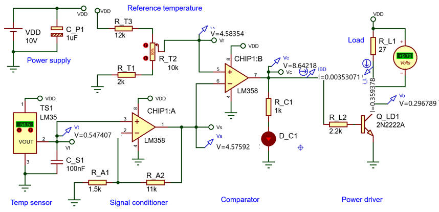
Fig. 3 is a Proteus simulation of the analogue Temp_cntl.pdsprj circuit.
|
|
|
Fig. 3. Simulation of the sensor conditioner and power driver values for an RL = 27 W heating element. VDD = 10 V. PL = 3.5 W. This simple BJT power driver generates 100 mW of power losses. |
PCB design KiCad
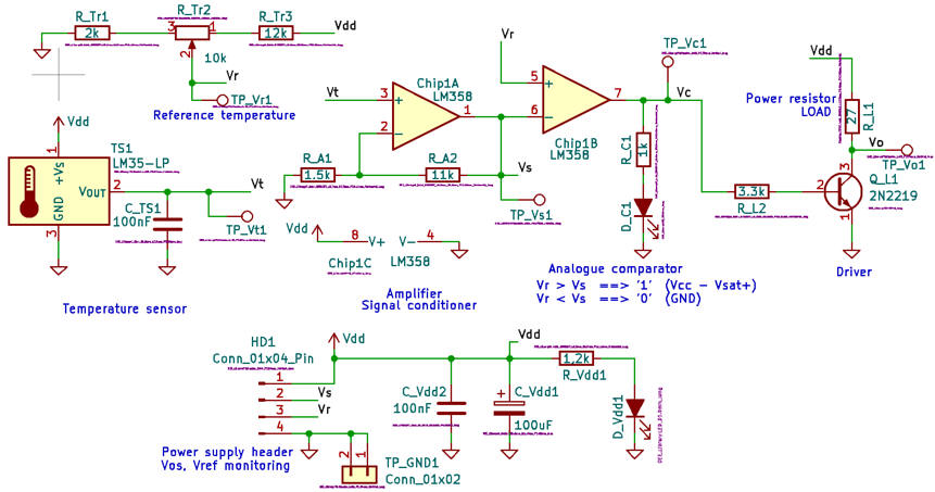
Prototyping is never solved in a single step, on the contrary, it takes some time and several drafts and calculations. These pictures and sketches are an example of what be the final prototype will be. The idea is to start adapting previous design using the same components libraries and design conventions and rules. Firstly, as shown in Fig. 4, we capture the schematic adding all the details on connectors, footprints and track sizes. Here we assume that power lines are 1 mm width and default cooper lines are 0.5 mm.
|
|
|
Fig. 4. Example printing of the schematic capture in KiCad. |
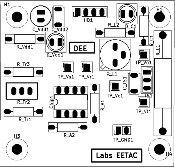
We continue placing al the components in the PCB tool before routing tracks, as shown in Fig. 5.
|
|
|
Fig. 5. Silkscreen represening component placement on the PCB. |
As shown in Fig. 6 we can render the 3D view to see how the board will look like.
|
|
|
Fig. 6. 3D representation. |
Kicad PCB files:
Temp_cntl_PCB_KiCad.zip
Current CSD and DEE KiCad symbols,
footprints and 3D tuned components:
symbols.zip,
footprints.zip,
3dmodels.zip.
PCB design Ultiboard
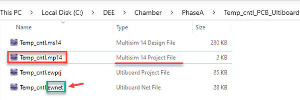
This is the same PCB using the EDA Multisim and Ultiboard from NI (Emerson): Temp_cntl_PCB_Ultiboard.zip project.
Paste the sample project given in the correct location and open it clicking the project file with ".mp14" extension to manage both the schematic and the PCB. Use the file extension ".ewnet" to transfer data from the schematic to the PCB and vice versa in order to keep both tools synchronised.
|
|
|
Fig. 7. Click the file extension "mp14" to work interactively with both the schematic and the PCB. |
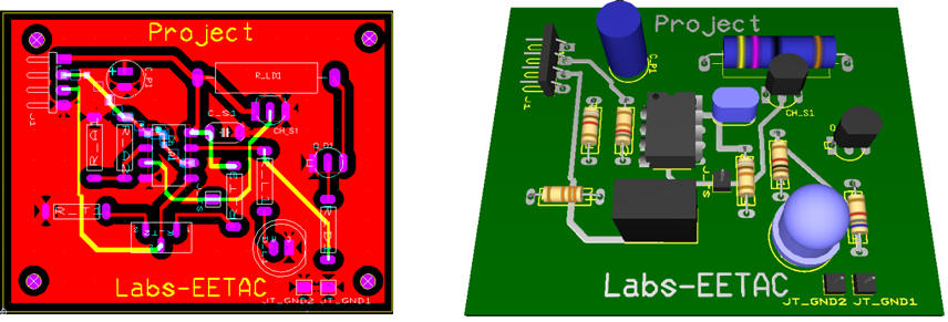
PCB design section the key idea is to find the correct footprint for every component while working concurrently inter-annotating the schematic in Multisim and the board in Ultiboard until completely routed.
|
|
|
Fig. 8. Circuit captured in Multisim and prepared as a PCB prototype using Ultiboard EDA tools. |
And this is how the board looks like once finished and ready for manufacturing.
|
|
|
Fig. 9. The same circuit captured in Multisim and prepared as a PCB prototype using Ultiboard EDA tools. |
PCB manufacturing and lab experimentation
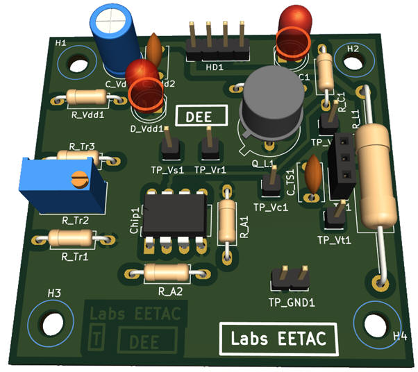
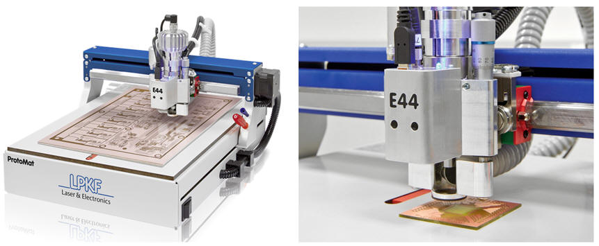
We fabricate the PCB using our Labs-EETAC machines. Gerber files for top (component) and bottom (solder) layers are extracted and processed by the computer-numerical-control (CNC) machine for PCB manufacturing.
|
|
|
Fig. 10. Computer numerical control (CNC) machine for PCB manufacturing available at EETAC labs: ProtoMat E44 from LPKF company. |
6. Laboratory experimentation and measurements
Let us validate the circuit performing measurements using laboratory instrumentation.
|
|
|
Fig. 11. Output waveform driving the resistor when Ts is aproximatelly TR |
|
|
||
|
|
Design phase B0: Arduino-based LCD temperature meter |
|
|
|
||
B0 specifications |
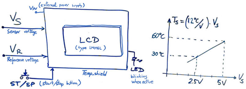
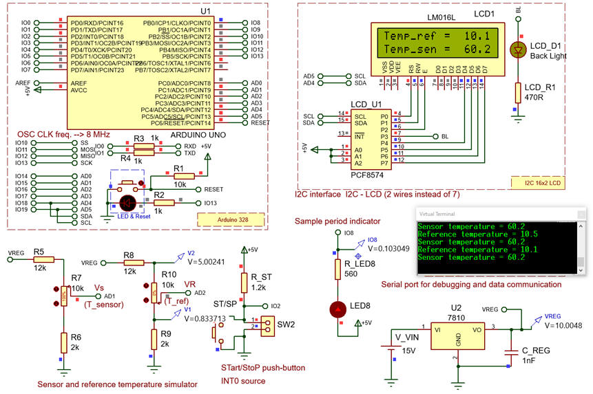
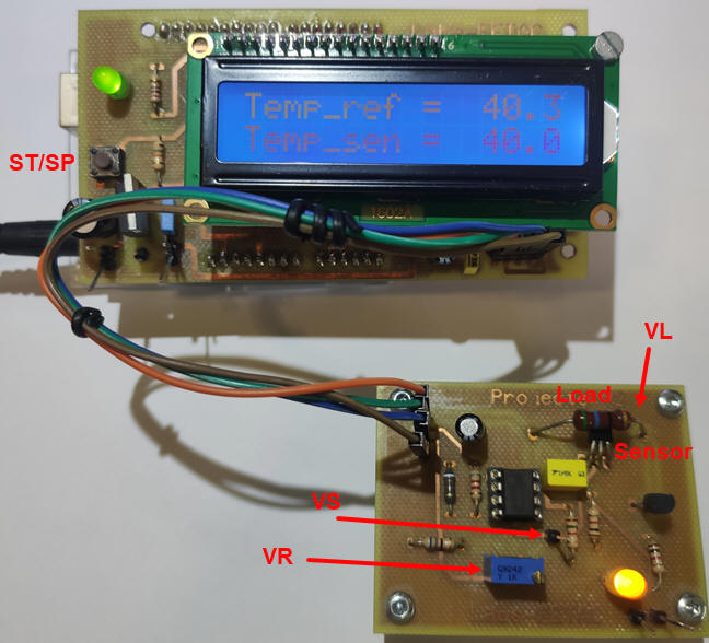
As a way to introduce Arduino microcontroller to the system, let us to display both temperatures TS (°C) and TR (°C) in a liquid crystal display (LCD) type LM016L with a simplified I2C iunterface.
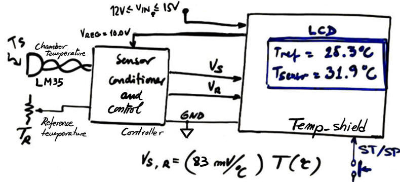
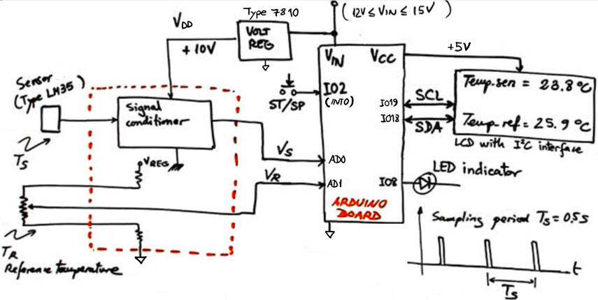
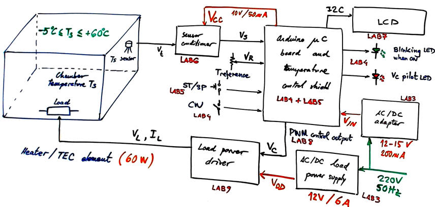
The Arduino input voltage VIN will be regulated to generate VDD = 10 V for powering the phase A analogue board. In the same connector J1, both voltages VR and VS will be available for the Arduino based LCD thermometer to display chamber TS (°C) and reference temperatures TR (°C).
We can imagine only positive temperatures up to 60 °C. Let us adjust the calibration curve to the standard analogue Arduino input range (VREF- = 0 V, VREF+ = +5 V).
Clicking a button will start/stop operation. A blinking LED will indicate activity.
2. Planning
Hardware
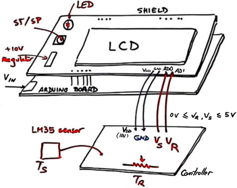
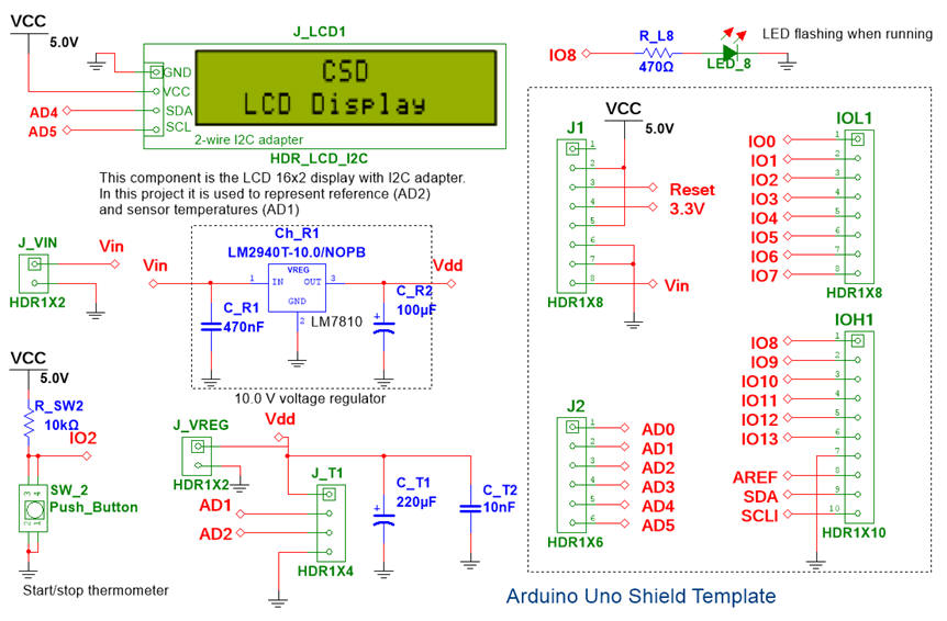
The LCD temperature meter will be adapted from the Temp_meter Arduino-based reference design (CSD P12): The display will be mounted in a shield along with the voltage regulator to supply VDD = +10 V.
|
|
|
Fig. 1. Shield for displaying the pair of temperatures of interest in an LCD. Controller's output VC and driver not shown. At this design phase B0, the digital system based on Arduino is only an auxiliary circuit, a thermometer for temperature monitoring. |
|
|
|
Fig. 2. Circuit adapted to our LAB6. VR and VS will be captured at AD0 and AD1 analogue inputs. |
Project location:
C:\DEE\Chamber\PhaseB0\(files)
C:\DEE\Chamber\PhaseB0\Proteus
C:\DEE\Chamber\PhaseB0\PCB
Software
The purpose of the software section is to acquire/measure/print a pair of temperatures on the LCD. Temperatures will be acquired at 2 Hz sampling frequency.
FSM-type programming style will be used to organise the C code, as done in LAB6 or in CSD (P10).
We copy and rename as Temp_shield the software code in Temp_meter because we use the same states. Study the state diagram and adjust the calibration curves considering the temperature range proposed for the chamber.
EMC
Study, discuss and calculate the additional components to make this circuit EMC compliance.
3. Development 4. Testing 5. Prototyping
Hardware
Software
The next picture shows how the software Temp_shield.pdsprj (unzip it in the correct location) is debugged using Proteus. The calibration curve is adjusted to the +10°C < VS, VR < +60°C.
|
|
|
Fig. 3. Temp_shield simulated to debug the software application before prototyping. |
Sensors and references can be modelled as ideal circuits or better replaced by potentiometers to easy the simulation convergence.
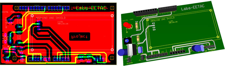
This is the Temp_shield.zip project captured in ModelSim and routed using Ultiboard EDA tools. If necessary, it can also be used as the thermometer and digital controller for experimenting in the next design phases.
|
|
|
Fig. 4. Temp_shield schematic in Multisim. |
|
|
Fig. 5. Temp_shield solder and component sides. |
Mount the project soldering the components and perform measurements to characterise how it works.
|
|
Fig. 6. Control system phase A soldered in PCB and running. |
6. Reporting
Documenting a project is basically organising and completing a report like the content of this page. In the same way, using pictures and diagrams you cam prepare some slides for an oral presentation. The basic four sections of your report are:
(1) Specifications. Use diagrams, graphics, bullet list, books and references of similar industrial applications.
(2) Planning phase B1. What circuits may work for each section (sensor, conditioner, references, comparator, power driver, temperature meter, etc.). Document each section in different sheets of paper. Several circuit alternatives may be proposed, each one with advantages and drawbacks.
(3) Developing & (4) testing the plan. Calculate the circuit proposed as a solution and simulate it to check that it works as expected in the specifications. Do it section by section. Take pictures or print graphics from simulators and analyse and discuss the results.
(5) Prototyping. Solder one section of the circuit at a time and measure how it works. Perform measurements and discuss how the circuit adjust to the specifications.
Additional questions (related to given sections of the project):
- How to modify the circuits to reach all our proposed temperature range from -5 °C to 60 °C while keeping a single VDD = 10 V power supply?
- Using the laboratory power supplies with current limiting protection, experiment and characterise the thermoelectric cooling element. Which range of temperatures are attainable? How to drive it?. How to complement it with the heater plate for obtaining high temperature plateaus inside the chamber?
|
|
||
|
|
Design phase B1: ON/OFF temperature control |
|
|
|
||
B1 specifications |
The same of design phase A replacing the analogue control by a digital ON/OFF control based on Arduino.
2. Planning
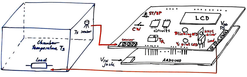
Our goal is the same set of initial specifications, thus we will start this phase B1 planning the new circuit so that the Arduino performs the ON/OFF digital control replacing the analogue comparator used in phase A. Microcontroller code will perform this simple control loop comparison operations to generate the driving signal for the heater and stabilise the chamber temperature (TS) to the given reference (TR). We will design a new temperature and control shield capable of driving 60 W of power into the chamber load element.
|
|
|
Fig. 1. Block diagram on the components included in this phase B1 based on an Arduino shield. |
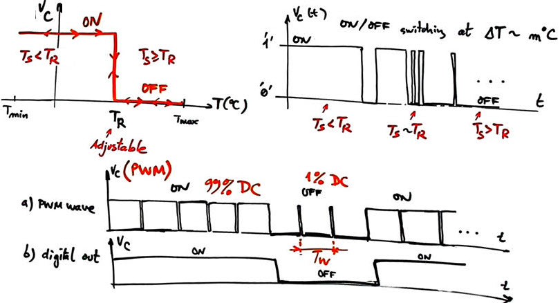
Indeed, as represented in Fig. 1, to generate this ON/OFF control signal, we can choose between HIGH and LOW output digital values, or equivalently 99% (HIGH) and 1% (LOW) PWM values. This is the purpose of the new CW (control wave) switch. In this way we can study how PWM are generated, advancing content for the next phase B2 on using PWM hysteresis control.
Hardware
As indicated in Fig. 1, we can adapt circuits from previous laboratory sessions to design the new shield. However, we may consider two steps to be able to advance testing hardware and software from the very beginning:
Step 1: use the same controller board and LCD shield in phase A. Cut the Vc PCB track (or add a jumper) from the comparator and generate this digital signal from a given Arduino output such IO9.
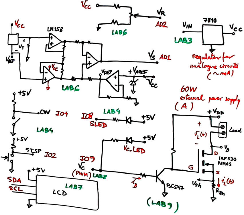
Step 2: Design the new temperature and control board, for instance the LAB9. Add the new elements: CW switch, VC pilot LED, new signal conditioner to adapt the full temperature range, new VIN = 10 V low-power voltage regulator (replacing the former in TO220 case), NMOS power driver.
A key element in this project is the load power supply, for instance 12 V - 5.5 A (65 W) for reaching the TEC's maximum DT. For this purpose, you can recycle an old portable PC power adaptor, or design a low-dropout linear regulator, or a Buck switching regulator for higher efficiency.
Finally, you may experiment driving both, the heater resistor and the TEC element to reach all the temperature span and to reduce transition times between reference points.
|
Fig. 2. Sketch of the new shield containing all the circuits. Only three terminal blocks are required to screw the sensor, the load and its power supply. |
Propose a calibration curve for this phase B1 circuit and propose schematics as shown in Fig. 3.
|
Fig. 3. Example of circuits inherited form previous laboratories to be calculated. |
Software
Let us adapt the previous phase B0 software adding a new state for implementing the control functions so that we can organise a FSM like the one proposed in LAB6.
|
Fig. 4. State diagram inherited from previous phase B0. It is modified to add the new ON/OFF control in the acquisition and processing loop. Processing activity is repeated for a brief fraction of time every sampling period. |
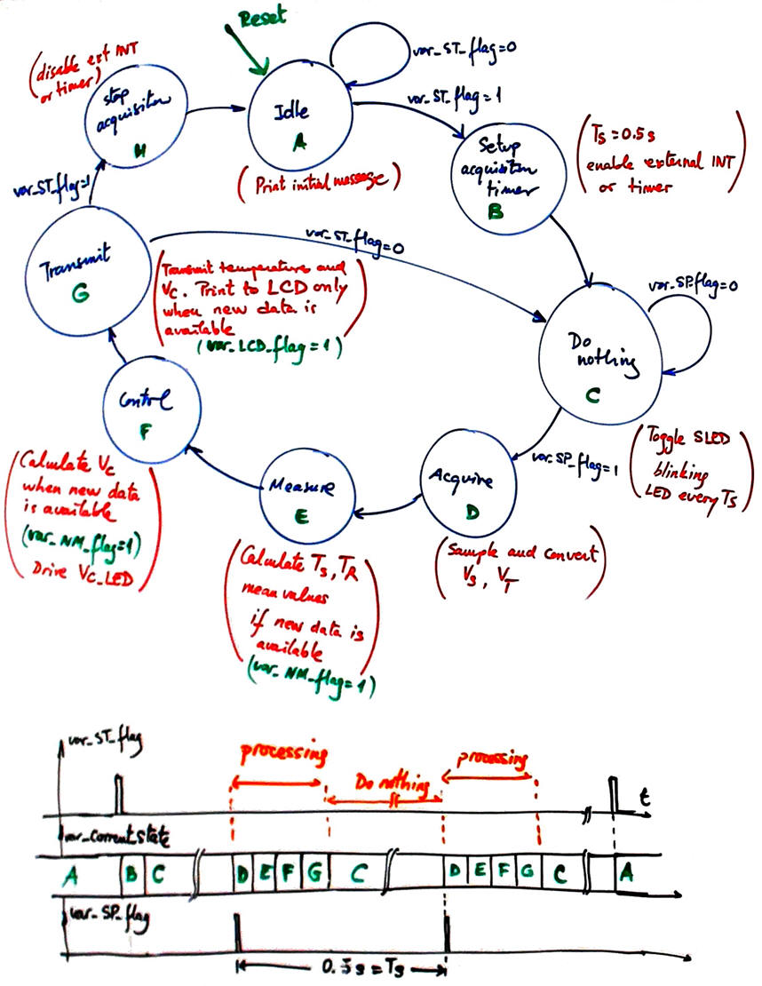
A way to spare some redundant processing time is to avoid calculations in measure and control states when the sensors are acquiring exactly the same values repetitively. Thus, we can add an indicator to detect new measurements var_NM_flag, in the same way var_LCD_flag was proposed to print on the LCD only when new data was available.
Poject location:
C:\DEE\Chamber\PhaseB1\(files)
EMC
Study, discuss and calculate the additional components to make this circuit EMC compliance. Add them to the PCB.
3. Development 4. Testing 5. Prototyping
Hardware
This is an example of Temp_control_shield.zip for this design phase B. Develop, test and prototype as done in phase A.
Software
The proposed translation to Arduino C code matching the state diagram in Fig. 3 is found in the zip file.
PCB design
Adapt the given Multisim and Ultiboard circuits in phase A to make a new PCB shield for this phase B.
6. Reporting
|
|
||
|
|
Design phase B2: PWM hysteresis control |
|
|
|
||
B2 specifications |
The same or similar to design phase B1, replacing the digital ON/OFF control by a hysteresis window.
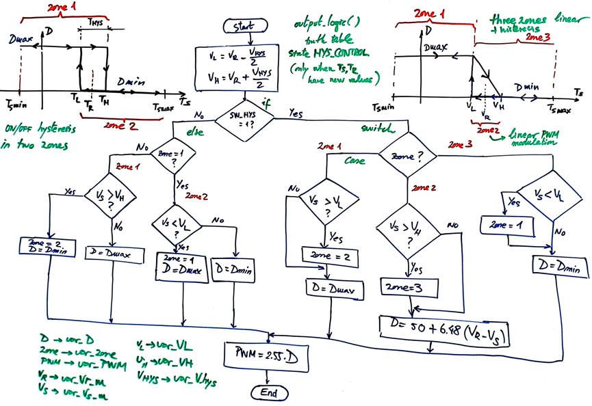
We can rename the switch control wave SW_CW from phase B1 to be switch hysteresis SW_HYS signal. When SW_HYS = '1' hysteresis control is applied, and when SW_HYS = '0' the previous ON/OFF equation is computed.
2. Planning
Hysteresis allows us the installation of a window of temperatures around TR that will reduce considerably the number of heater or cooler device switching operations. For example, in A mode, the control system will order the heater to switch on when the temperature TS drops below TL, but will prevent it to turn it off until the temperature TS rises above TH.
|
|
Fig. 1. We propose two hysteresis functions for controlling the chamber's temperature. The mode A is the typical one in two control zone and running the duty cycle at ON/OFF with DMAX/DMIN. The mode B control equation includes the linear zone 2 in the hysteresis window applied when the chamber is heating. The evolution of Ts(t) represents only an approximation; thus experimenting in the laboratory we can characterised the chamber as a transfer function for designing more complex control systems. |
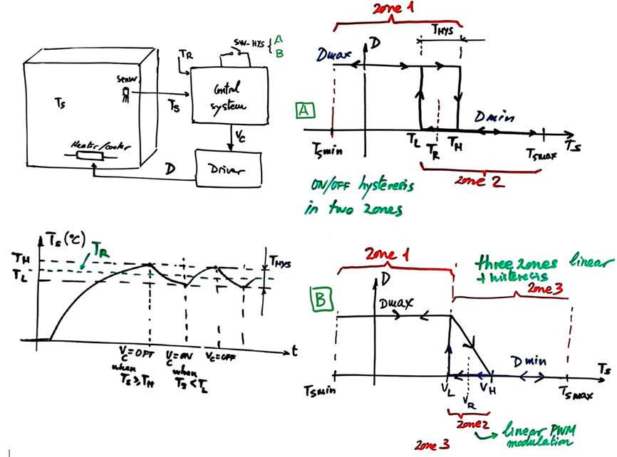
In mode B, we can use comparisons for segmenting the control in three zones. Thus, in control zone 2 the equation can be calculated in function of the design parameters TR and THYS as shown in Fig. 2.
|
| Fig. 2. Zone 2 linear equation. |
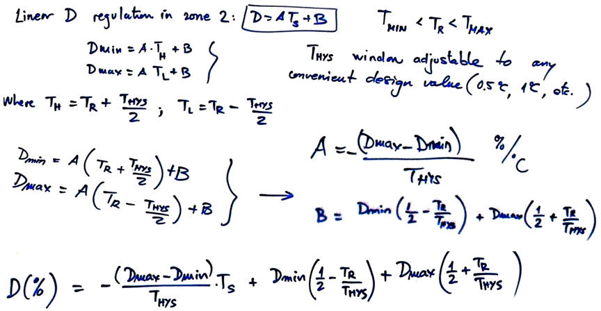
Fig. 3 shows the duty cycle equation and how to calculate it from the acquired voltages representing temperatures.
|
|
|
Fig. 3. Duty cycle equation and a proposed example in the control zone 2. |
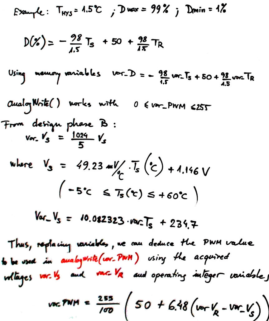
For instance, if THYS = 1.5 °C, DMAX = 99%, DMIN = 1%, considering a reference TR = 30 °C, the equations in the control zone 2 shows when the sensor is at :
- TS = 30 °C, var_Vs = 537, var_D = 50; var_PWM = 128, var_TS = 30.0
- TS = 29.25 °C, var_Vs = 529.6, var_D = 2; var_PWM = 5, var_TS = 29.25
- TS = 30.75 °C, var_Vs = 544.73, var_D = 100; var_PWM = 255, var_TS = 30.75
Software
The new control equations will be implemented in the HYS_CONTROL state replacing the phase B1ON/OFF equations. To save computing time, this processing will be performed only when new temperature values are available.
|
|
| Fig. 4. Flowchart to be solved in HYS_CONTROL state. Depending on the SW_HYS read value, we can perform the typical hysteresis control, or the modified one with linear PWM modulation in the hysteresis window. |
Hardware
The circuitry will be the same as in previous phase.
Project location:
C:\EMC\Chamber\PhaseB2\files)
3. Development 4. Testing 5. Prototyping
Hardware
We have only renamed the SW_CW to be SW_HYS to assign it control equations A or B in Fig. 1.
Software
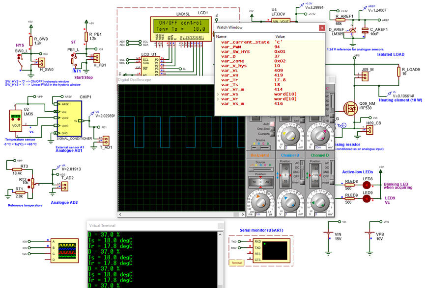
This is the new Temp_control.zip complete circuit modelled and running in Proteus.
|
|
| Fig. 5. Example picture of the circuit running in Proteus showing the watch window for debugging purposes. |
PCB
No need to make any change in the PCB, it is the same as in phase B1. In this phase B2 we update only the firmware of the controller.
6. Reporting
|
|
||
|
|
Design phase C: Power supply |
|
|
|
||
C specifications |
Our goal is to power the controller equipment. Design a 12V - 6A power supply for the circuit. We have two options: (a) a linear low-dropout voltage regulator. (b) a swithing regulator.
|
|
||
|
|
Design phase D: Communication interfaces |
|
|
|
||
D specifications |
Our goal is to command and monitor the equipment using a wireless interface and computer or Android appplications. We can also implement a virtual instrument (LabWindows CVI, LabView) to specifiy temperature profiles and represent all the data.
| Home Contact Electronic devices and companies Books Magazines Instruments Digsys Library EETAC DEEL |

|
|
| Web activa des de 01/2023, @ F. J. Robert. Web editat amb Microsoft Expression Web 4. El contingut és material de referència per al disseny d'equips electrònics. Llicència:Reconeixement 4.0 Internacional de Creative Commons |