|
|
Bachelor's Degree in Telecommunications Systems and in Network Engineering. Bachelor's Degree in Aerospace Systems Engineering |
|
|
Pulse width modulation (PWM), D/A conversion, analogue outputs, analogue filters |
| 1. Specifications | Planning | Dev. & test | Prototype | Report |
Our first goal is to generate analogue voltages using (1) PWM techniques and (2) specific D/A chips. For instance, DC, triangular, ramp and sinusoidal waveforms at different frequencies.
We also aim conditioning analogue outputs (1) filtering high frequency noise associated to the D/A conversion process and (2) generating current outputs to drive devices such analogue panel needle meters or 4-20 mA current loops.
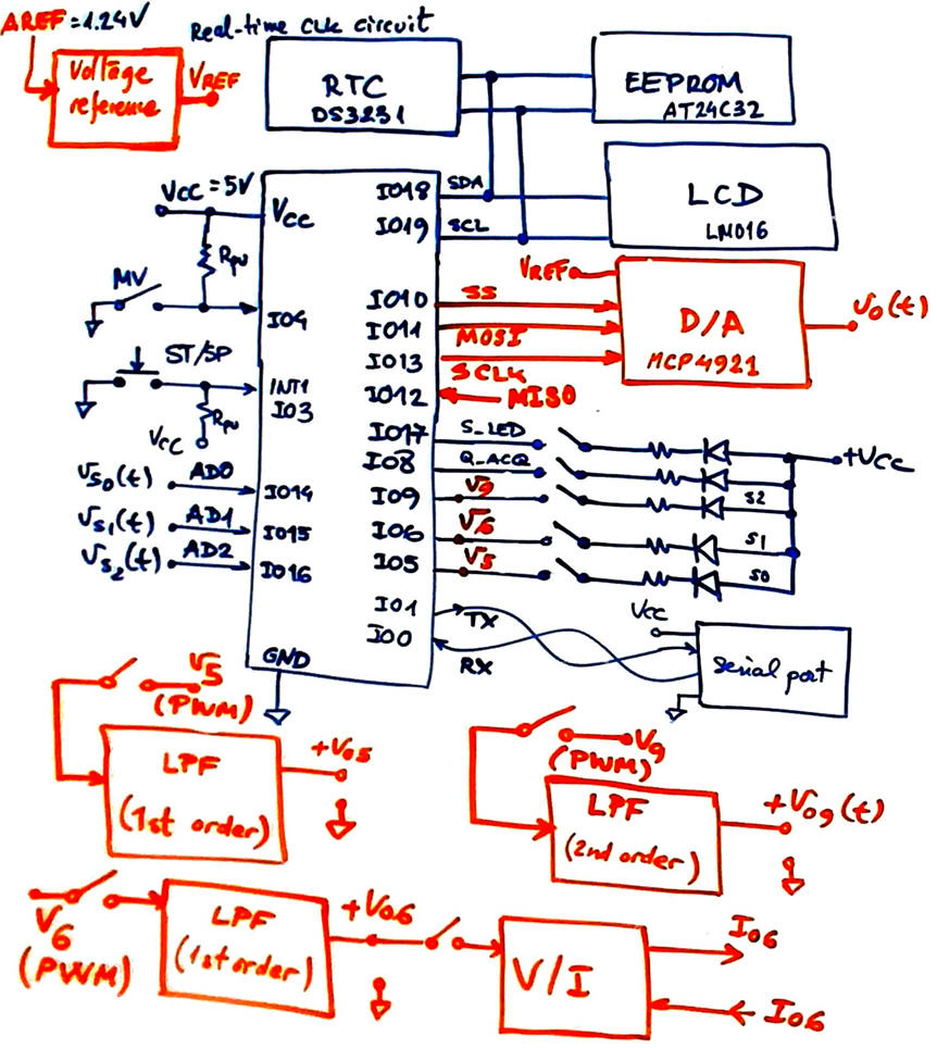
We can complement the previous LAB7 circuit adding a real-time clock circuit chip (RTC) and also an EEPROM memory for saving data and parameters permanently.
 |
| Fig. 1. Block diagram of several analogue output circuits from Arduino. |
Single power supply 5V
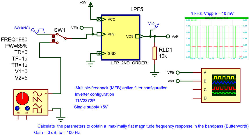
Active 0dB first-order filter (-20 dB/dec), 5V rail-to-rail operation, cutoff frequency fC= 100 Hz.
Active 0dB second-order Butterworth response filter (-40 dB/dec), 5V rail-to-rail operation, cutoff frequency fC= 100 Hz
Modify and enhance the previous application LAB7 so that in a new state (waveforms) the following voltages and currents are calculated:
- Output VO6 generates the same analogue voltages acquired at VS1
- Output VO5 drives the needle panel indicator coil from 0 to 100%
Drive a 1 mA = IFS needle panel indicator from VO9.
Analogue values will update every TD = 2 s (distribution CLK period).
PWM signals
Pulse-width modulation Wikipedia page.
Digital to analogue converter peripheral
Digital-to-analog converter Wikipedia page.
Low-pass filer design
Wikipedia LPF reference.
Example of passive and active filter circuits.
Other references: Thomas, R. E., Rosa, A. T., Toussant, G. J, "The Analysis and Design of Linear Circuits", 7th ed, John Wiley & Sons, Inc., 2012
TI, TLV237x: Rail-to-Rail input and output operational amplifiers with shutdown
TI, SBOA231: Single-supply, 2nd-order, multiple feedback low-pass filter circuit
TI, SNOA224A: AN779 National: A basic introduction to filters - active, passive, and switched capacitor
TI, SLOA049D: Active Low-Pass Filter Design.
Proteus: an introduction to active filters (ref.)
Current sources and voltage to current converter.
Let us drive a moving coil panel meter type SD38/0-1MA. as shown in Fig. 2. The meter scale can be customised to any quantity and span as shown in this reference page.
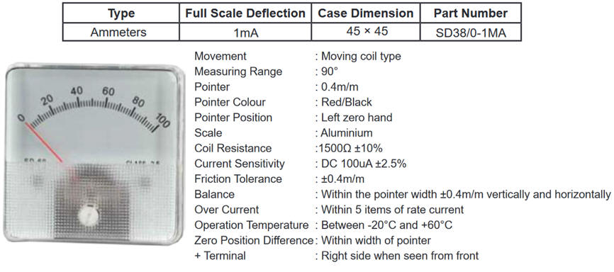 |
| Fig. 2. Panel analogue needle meter. |
Let us drive the coil with a voltage controller current source. This are useful references from Texas Instruments on the design of Howland current sources (1), (2).
Real-time clock and EEPROM.
Using the I2C bus, it is easy to add other convenient modules to our prototyping board. For instance, the DS3231 RTC Module that also includes a 32 kbit EEPROM memory.
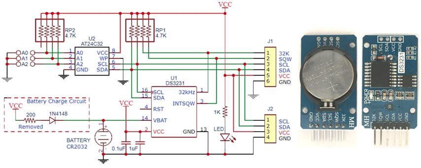 |
| Fig. 3. DS3231 RTC Module. |
Topics in EMC
| Specifications | 2. Planning | Dev. & test | Prototype | Report |
Hardware
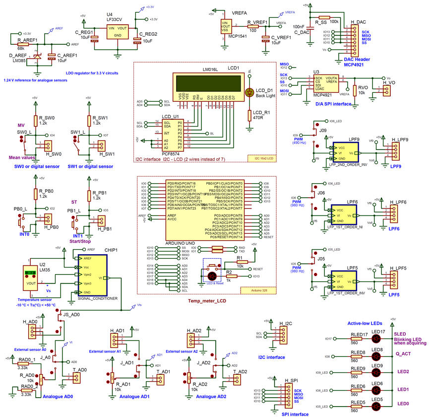
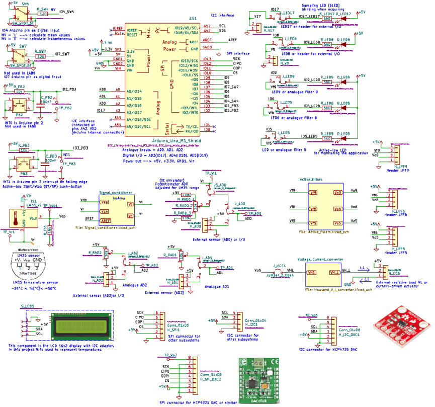
The idea is to continue expanding our previous project LAB7 adding jumpers to three specific pins so that they can be available as analogue outputs disconnecting the LED.
For example, we can connect a D/A converter type MCP4921 by means of the SPI bus.
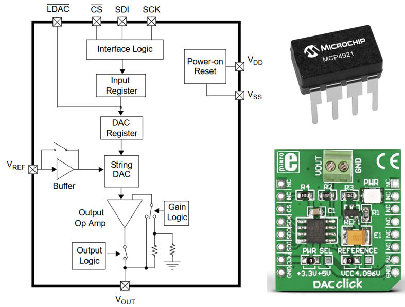 |
| Fig. 4. MCP4921 breakout (12-bit D/A) for Arduino (ref. including the circuit). |
Or instead, in a similar way, an external D/A type MCP4725 can be connected by means of the I2C bus.
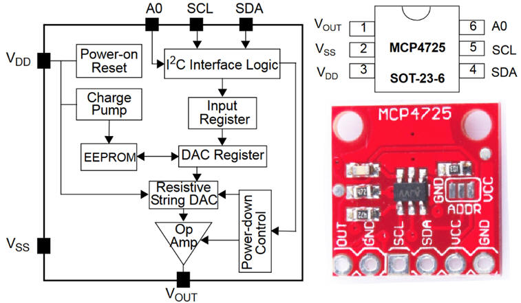 |
| Fig. 5. MCP4725 breakout board (12-bit D/A) for Arduino or Raspberry Pi circuits. |
Arduino circuits will include the D/A and the analogue filters.
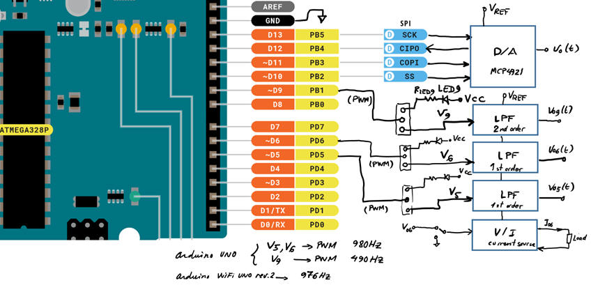 |
| Fig. 6. Arduino connections to add analogue filters to the three PWM outputs 5, 6, and 9, and also an MCP4921 breakout board. |
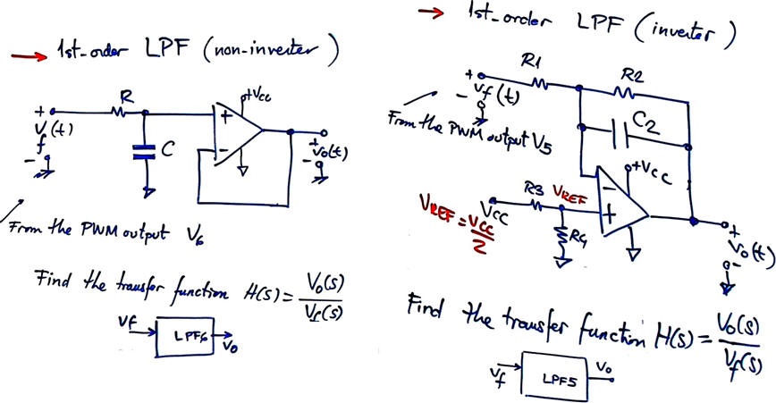
To design the 1st-order LPF5 and LPF6, as shown in Fig. 7 we can choose between two models based on OpAmps. We need to analyse its transfer function H(s) in the Laplace domain in order to locate the pole in the required position on the real axis of the left half of the s-plane diagram.
 ç ç |
| Fig. 7. First-order active LPF. |
To design the 2nd-order LPF9 we can choose a multiple-feedback configuration as represented in Fig. 8. We need to calculate its transfer function H(s) and be able to locate the conjugate poles so that the frequency response is maximally flat in the bandpass (Butterworth response).
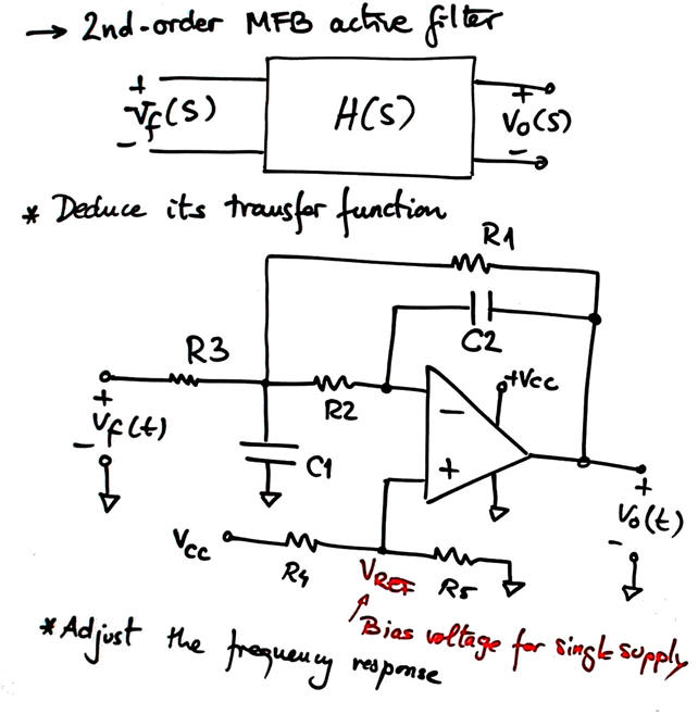 |
| Fig. 8. This is a proposed second order low-pass filter (-40 dB/dec). |
To design a voltage to current converter (or transconductance amplifier) we can use the Howland current source shown in Fig. 9 and adjunct it to our requirements to drive the needle panel indicator proposed in Fig. 2.
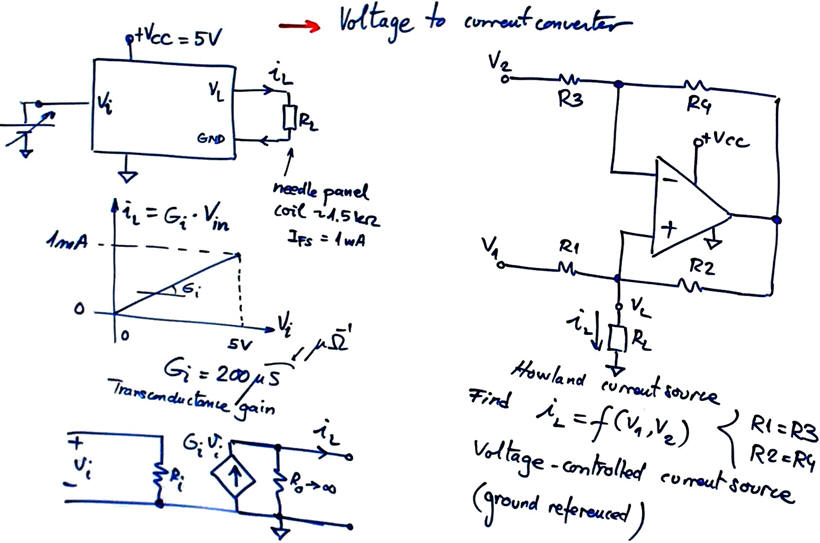 |
| Fig. 9. An example idea on the design of a voltage controlled current source. |
Software
Function analog_write() function to generate analogue signals.
Interfacing SPI MCP4921 chip, example page.
Interfacing I2C MCP4725 chip, example page.
To start experimenting with analogue output generation we will add another state "waveforms" to our FSM.
Project location:
C:\DEE\LAB8\Temp_LCD_DA\(files)
| Specs | Planning | 3. Dev. & 4. Test | Prototype | Report |
Hardware
Fig. 10 shows the virtual simulation first-order filters: filters_freq_response_1st_order.pdsprj.
This is the virtual simulation second-order filters: filters_freq_response_2nd_order.pdsprj.
 |
| Fig. 10. Second order filter captured as a subcircuit in Proteus. It can be tested using instruments and advanced graphical analysis. To obtain the filter frequency response we can simplify the OpAmp using it ideal model. |
This is the virtual simulation of the voltage to current converter: Howland_current_source.pdsprj.
Fig. 11 shows the new board enhanced from LAB7 including the digital to analogue new blocks. It includes the software program Temp_meter_LCD_DA.zip to be enhanced in this laboratory to generate analogue output signals.
 |
| Fig. 11. Hardware application captured in Proteus ready for simulation after adding new FSM states. |
Software
We have to add a new state to generate correctly the D/A signals at the given distribution CLK.
 |
| Fig. 12. Modified state diagram. |
Using Proteus we have a way to test and adjust filters gain and cutoff frequencies selecting resistors and capacitors.
|
|
| Fig. 13. Simulation running and watching waveforms and RAM variables. |
| Specs | Planning | Dev. & Test | 5. Prototype | Report |
In this section we go from computer simulations to the laboratory. We can continue enhancing the previous LAB7 board adding other components: the analogue filters and the Howland current source. We can use the jumpers to disconnect the LED outputs and connect the filters.
 |
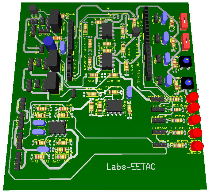
|
Fig. 14. KiCad top schematic capture. See the full schematic and its additional sheets opening the project. We include many headers for experimenting and for connecting signals to instruments. |
The PCB implementation using KiCad: LAB8_PCB_Temp_meter_LCD.zip. Additional header connectors will allow us to connect D/A converter breakout boards such in Fig. 4 (SPI) and Fig. 5 (I2C) directly to the specialised Arduino pins.
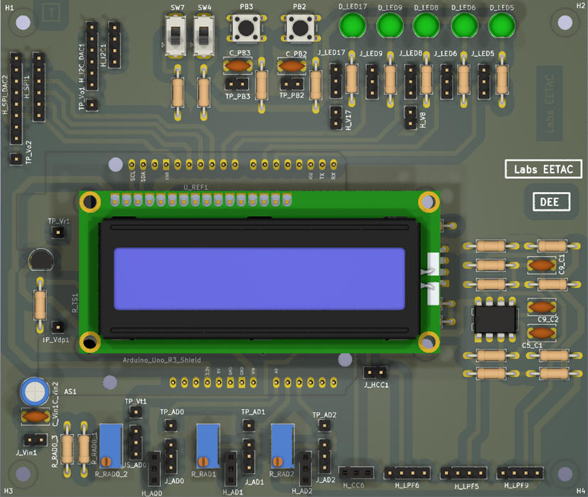  |
| Fig. 15. Top and lateral views of the PCB. |
NOTE: Current CSD and DEE KiCad symbols, footprints and 3D tuned components are available in these three libraries: symbols.zip, footprints.zip and 3dmodels.zip, to be unzipped and placed in the corresponding 3rdparty user directory. Basically, in this introductory level the idea behind tunnig components is to enlarge their pads for easy soldering.
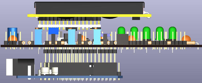
Fig. 16 is yet another version of the PCB using Multisim - Ultiboard: LAB8_PCB_v2.zip.
 |
| Fig. 16. 3D view of the prototype board completely wired. Only the cooper GND plane is yet to be connected. |
Experimentation and measurements
| Specs | Planning | Dev. & Test | Prototype | 6. Report and postlab assignments |
This web page in itself is an example of report consisting of five sections.
Additional questions:
- Modify and enhance the application so that in the new state (waveforms) another voltage is calculated: output VO9 generates an analogue voltage corresponding to the mean value of the three analogue inputs.
- While the FSM is running, generate an audible 1 kHz sinusoidal waveform output VO from the SPI D/A converter.
Annex: Fourier series of a PWM waveform
We can represent a rectangular PWM waveform using a Fourier series, an infinite number of harmonic.
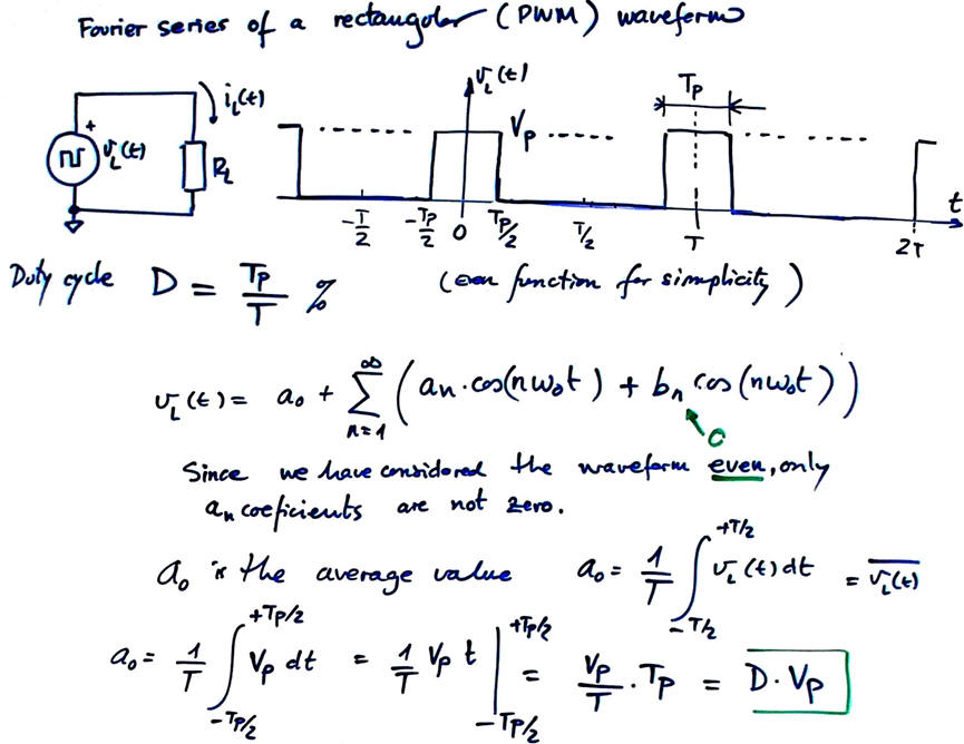 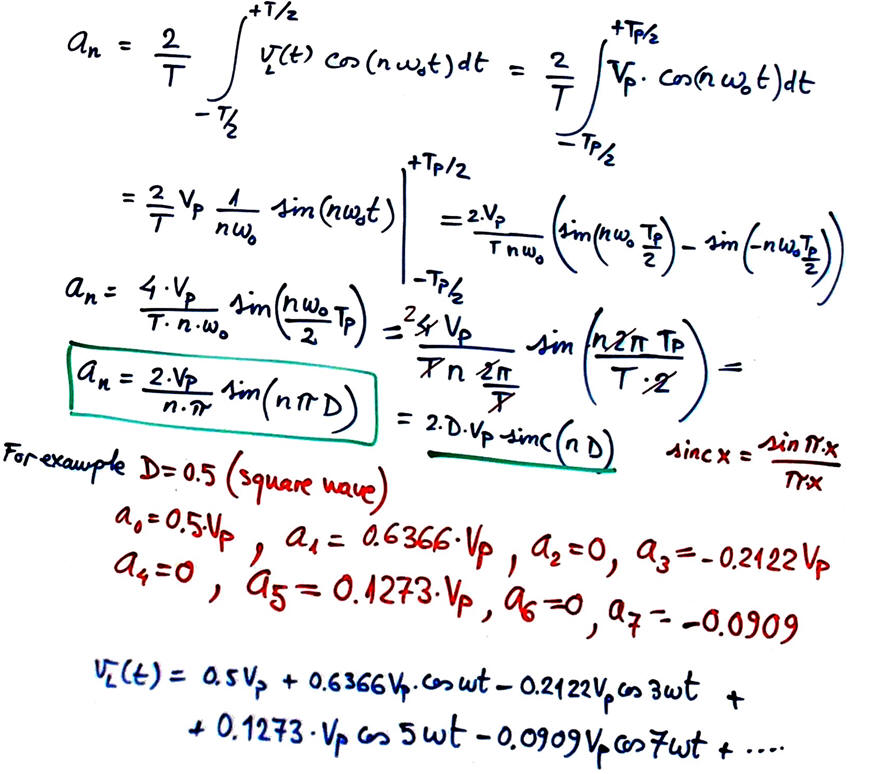 |
| Fig. 1. Fourier representation of a PWM waveform (ref.) |
In this way, it is easy to visualise how choosing correctly the cutoff frequency of a LPF we can generate the waveform mean value.
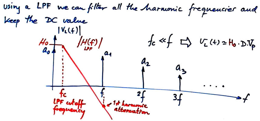 |
| Fig. 2. Mean value of the PWM waveform filtering all the harmonics. |
| Home Contact Electronic devices and companies Books Magazines Instruments Digsys Library EETAC DEEL |

|
|
| Web activa des de 01/2023, @ F. J. Robert. Web editat amb Microsoft Expression Web 4. El contingut és material de referència per al disseny d'equips electrònics. Llicència:Reconeixement 4.0 Internacional de Creative Commons |