|
Laboratory |
Laboratory 6: designing finite state machines (FSM) [P6] Control system for our classroom luminaires |
[14/11] |
| This is the group post lab assignment PLA6_7 to be submitted at Atenea before the due date. Study and execute in your computer this LAB6 and the next LAB7 lab tutorials before attempting to solve this post lab assignment. |
2.6.2. Control system for classroom luminaries
| 1. Specifications | Planning | Developing | Test functional | Test gate-level | Report | Prototype |
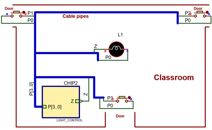
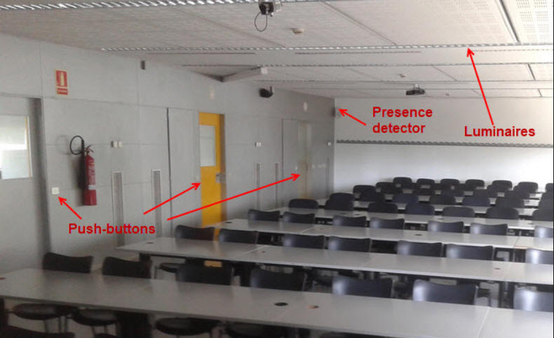
Let us define the product requirements of the system Light_Control for the classroom luminaires composed of 6 lines of 4 fluorescent lamps each (36 W). After two consecutives clicks the lamp turns ON, and when clicking for the third time it turns OFF. The CLK signal to synchronise the application is 200 Hz. Let's use the FSM design approach targeting a programmable device like a CPLD or a FPGA. Fig. 1 shows the project's symbol and layout.
 |
|
|
|
Fig. 1. Example of a classroom layout. Any push-button can switch ON and OFF the lamps.
This is a Proteus realisation of the FSM using classic chips that functions in a very similar way switching ON and OFF the lamp clicking only one time. |
In Fig. 2 we represent sketches on how to interface buttons and power loads to a low-power digital circuit. See how any number of buttons can be connected by means or an OR function to a single input B. If the buttons are active-low, such as B_L, can be converted to active-high using a NOT gate.
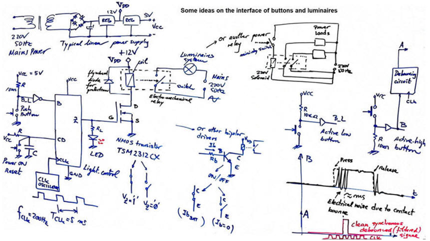 |
| Fig. 2. Proposed schematic. See in this Proteus circuit electromagnetic relays and power drivers and how they are used to adapt power levels. To run this machine, we need clean digital pulses when clicking and releasing keys or push-buttons, this debouncing_filter perform this filtering function. |
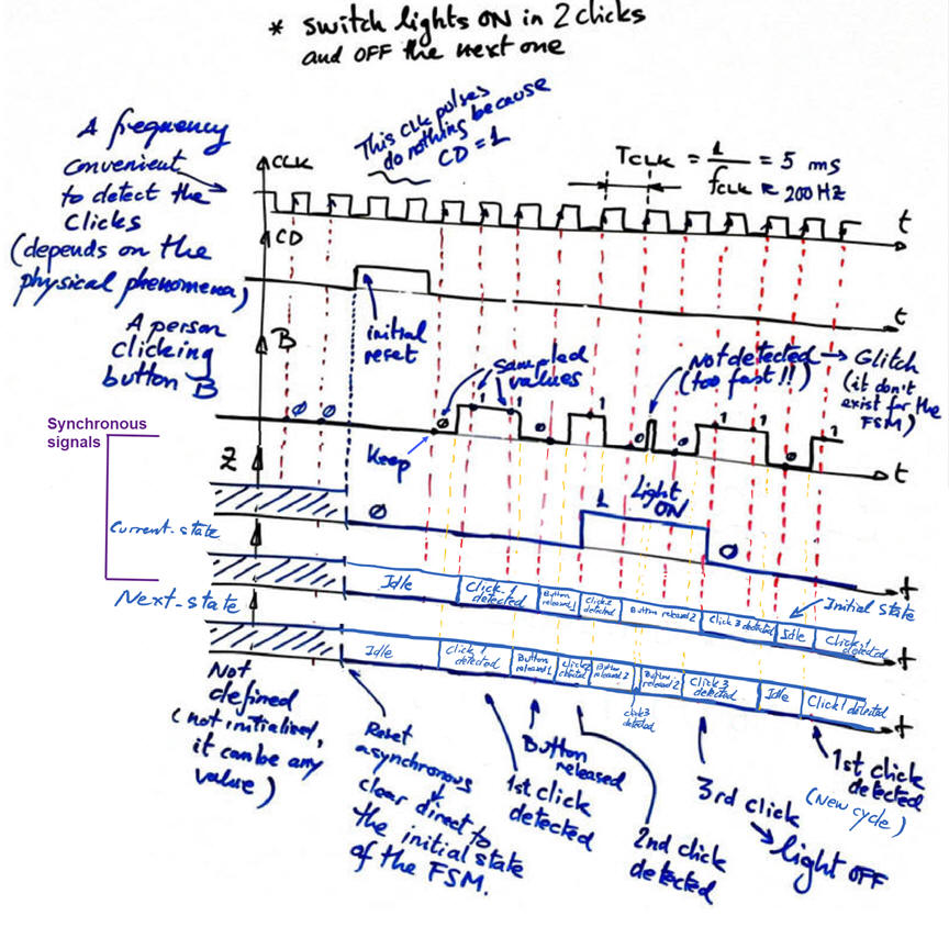
Fig. 3 shows an example timing diagram where the idea of clicking the button twice to turn on the light is described.
 |
|
|
Fig. 3. This is an example timing diagram. The evolution of the internal current and next state signals are also depicted. |
|
|
Indeed, before going ahead with the planning, it is interesting
to describe this application specifications in several
design steps and phases, as if it were simply another
proposed
PLA6_7. In this
way you can imagine how this application can go far
beyond a simple laboratory tutorial session. For
example:
Design phase #1: basic features. FSM architecture and current state encoding, asynchronous reset (CD), system clock (CLK), sampling input values, synchronous systems, maximum speed of operation, etc. - Design step #1. Consider an initial circuit only with the button B and the output Z (this LAB6) - Design step #2. Design the power drivers for the luminaries. - Design step #3. Add the debouncing filter for conditioning the push-button noisy signal. Design phase #2: advanced features, datapath, dedicated processor (presence sensors, timers, security, etc.) - Design step #1. If the second push-button click in not detected in less than 20 seconds from the first click, the machine will reset. - Design step #2. Add a presence sensor like the typical PIR motion detector HC-SR501.to save energy. If no one is detected in the classroom in 4 minutes, the luminaries will turn off. - Design step #3: Design a CLK generator to obtain all the necessary CLK signals from the 50 MHz target board quartz crystal oscillator. Deduce the number of D_FF required for this subcircuit. Design phase #3: PCB design and laboratory measurements. Integrate all the components in a single PCB so that the application can be controlled using the 40-pin flat wire from (1) the DE10-Lite board or from the CSD_PICstick. |
| Specifications | 2. Planning | Developing | Test functional | Test gate-level | Report | Prototype |
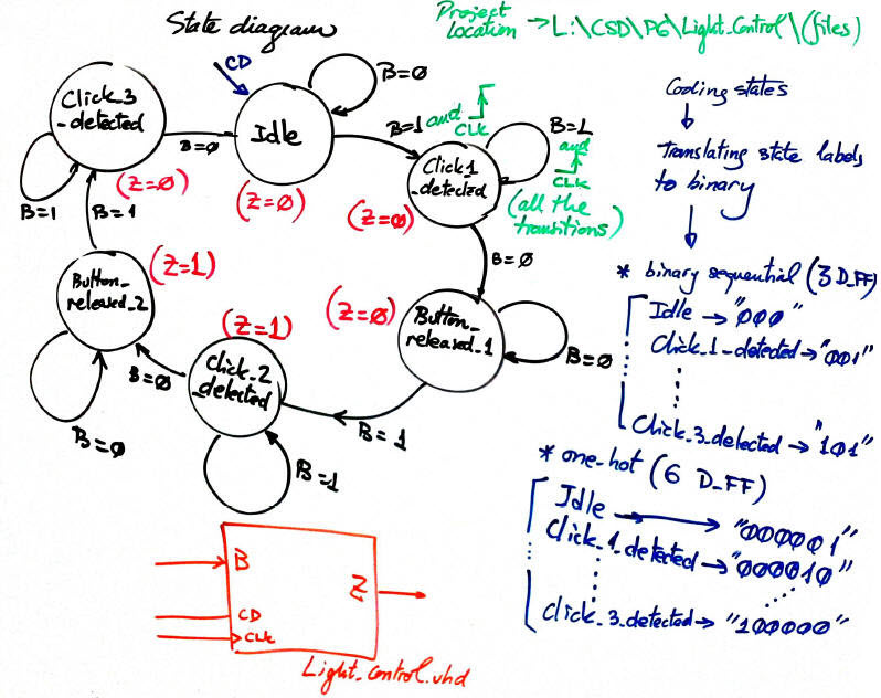
We will use the FSM architecture for this squential system. Infer and draw a state diagram as represented in Fig. 4 so that the system has enough internal memory to remember the three consecutive clicks of the same push-button.
 |
|
|
|
Fig. 4. The proposed state diagram. |
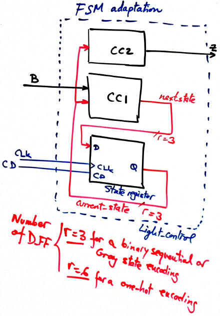
Adapt the general FSM architecture to this problem.
|
|
Fig. 5. The adaptation of the general FSM architecture to this problem. In VHDL the translation will consist of a single file with three processes. |
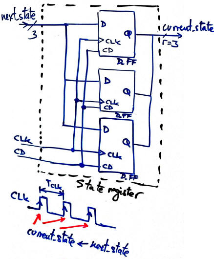
Draw the state register based on D_FF. How many D_FF registers will be required in this project if coding the internal states in binary (sequential), Gray or one-hot?
|
|
Fig. 6. The state register based on D_FF represented when r = 3, for instance for coding states in binary sequential or Gray. In VHDL the state register will be translated in a behavioural way as a process as shown in the D_FF tutorial. |
Write the CC1 and CC2 truth tables.
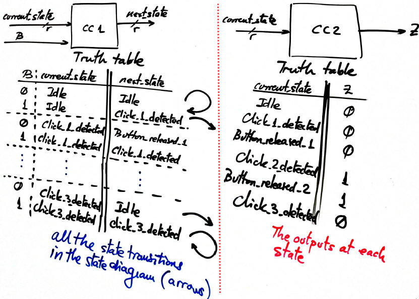 |
Fig. 7. CC1 and CC2 truth tables for solving state transitions and outputs. The key idea for solving these logic functions and to make it simple is sectioning the truth table by states (VHDL CASE statement). In addition, we have the great advantage of being able to use labels instead of logic values to represent current and next state signals. |
Describe the truth tables using a behavioural interpretation as in plan B. The flowcharts in Fig 8 are ready for translation to VHDL using processes.
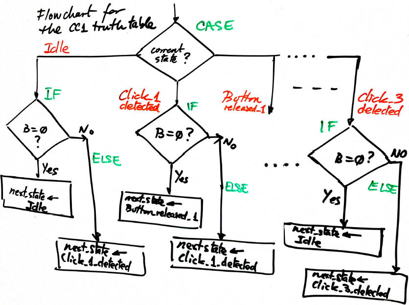 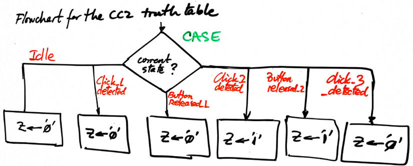 |
Fig. 8. Flowcharts for the CC1 and CC2 truth tables in Fig. 6. Green colour shows the statement that is the direct translation to VHDL. |
The project is solve in a single VHDL file applying plan C1, because we have decided to describe the three blocks conforming the FSM architecture as processes instead of independent components.
Project name Light_Control_prj
Project location:
C:\CSD\P6\Light_Control\(files)
| Specifications | Planning | 3. Developing | Test functional | Test gate-level | Report | Prototype |
This is a full video sequence rec. to facilitate these synthesis and testing phases. The idea is to translate the flowcharts from the plan above (Light_Control.vhd).
Select a target device, start a new synthesis project.
Choose the state encoding style (sequential (radix-2), Gray, one-hot, etc.) and run the EDA tool to inspect the RTL schematic and the interpretation of the state diagram.
Check the number of D_FF. For instance, if we select sequential state encoding style, inspect the circuit in Fig. 9 and explain what resources may be CC1 and the CC2 circuits.
|
Fig. 9. RTL schematic produced by a synthesis tool (click the icon to expand the picture). This diagram may differ depending on the EDA tool used. |
Let's inspect the technology view to be able to count again the number of D_FF registers used.
 |
|
Fig. 10. Example of a technology view where the number of D_FF are displayed connected to logic cells that implement CC1 and CC2 combinational circuits. Three D_FF are required when coding states in binary sequential or Gray. Discuss this picture and infer which wires represent the next state to go and the current state of the FSM, what block is the CC2? (click to zoom). |
Annotate the percentage (%) of the target chip occupied or the number of logic elements used. Another option is to locate the used resources using the Chip Planner tool.
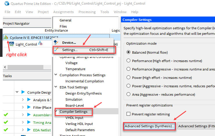
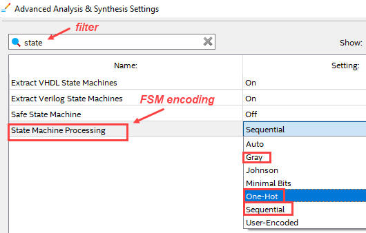
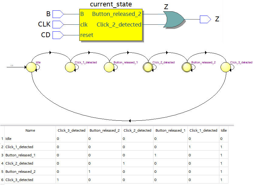
Alternatively, as shown in Fig. 11, if we choose one-hot code for representing states (or "writing our state labels in silicon"), the circuits in Fig. 12 and Fig. 13 are synthesised. They contain six D_FF and a different number of logic cells are used for implementing CC1 and CC2.
  |
|
Fig. 11. Selecting how to encode states in Quartus Prime. |
We can view the FSM state diagram, its transitions and encoding.
 |
|
Fig. 12. State diagram using one-hot encoding |
 |
|
Fig. 13. Technology view picture. (Click to zoom). |
| Specifications | Planning | Developing | 4. Test functional | Test gate-level | Report | Prototype |
This in Fig. 14 is the VHDL testbench schematic that we have in mind to run simulations for synchronous circuits.
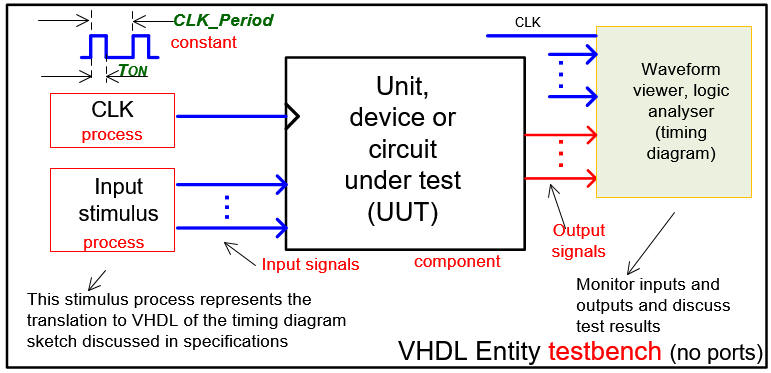 |
| Fig. 14. Testbench where to make it easy the CLK is another concurrent process. (visio) |
Generate from Quartus Prime the VHDL testbench fixture skeleton in Fig. 14. Rename it and move it to the project folder.
Copy from this example file Light_Control_tb.vhd only the stimulus activity described in the two processes and also the constant CLK_Period.
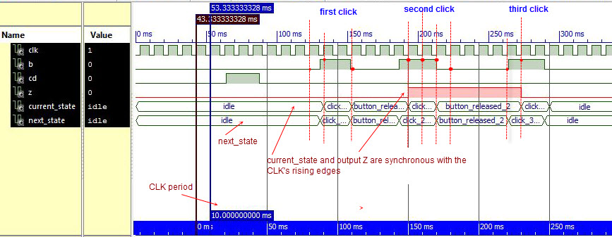
Start and run a functional simulation project using ModelSim to verify that the device operates like expected in the initial timing diagram sketch in Fig. 3. Going down one level in the hierarchy to pinpoint the instance i1, drag to the wave diagram the internal signals current_state and next_state.
Fig. 15 capture shows how it works presenting at the same FSM internal signals current_state and next_state to help debugging for finding any error.
|
|
|
Fig. 15. Example of a functional simulation. Note how meaningful is to represent as well the current_state and the next_state signals of the UUT. |
| Specifications | Planning | Developing | Test functional | 5. Test gate-level | Report | Prototype |
Gate-level simulations in ModelSim
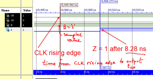
Using the same testbench, Fig. 16 shows a given transition in the gate-level timed simulation. In the real circuit (technology view) it takes some time to propagate signals from inputs to outputs.
|
|
|
Fig. 16. Gate-level simulations at a given CLK transition and the synthesiser timing analyser. Target chip used is Cyclone IV. |
Quartus Prime timing analyser
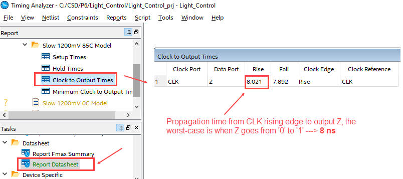
Fig. 17 shows also timing analysis results when using MAX10 chip.
|
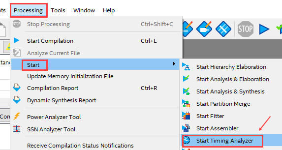
a) Start timing analyser at "Processing --> Start Timing Analyser"
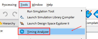
b) View results at "Tools" ---> Timing Analyser
c) Run the task generate "Report Datasheet" and select the measurement Clock to Output times |
|
Fig. 17. In this circuit, targeting a MAX10 chip, we can measure a tCO = 8 ns, representing a system CLK maximum frequency of operation fMAX = 125 MHz. |
| Specifications | Planning | Developing | Test functional | Test gate-level | 6. Report | Prototype |
Follow this rubric for writing reports.
| Specifications | Planning | Developing | Test functional | Test gate-level | Report | 7. Prototype |
Tutorial continuation: Prototyping. Board DE10-Lite. Hardware circuits for CLK circuits, LED, 7-segment displays, buttons and switches. Pin assignment, programmer.
Once the circuit works in the simulator, the idea is to continue the project development in the laboratory programming the target chip (CPLD or FPGA) with the project file. We can experiment and characterise the prototype using instrumentation.
In our lab, there are several training boards populated with Xilinx, Lattice Semiconductor and Intel chips. Projects can be easily adapted to specific boards attending logic levels, oscillators, switches, displays, etc.
Intel Terasic DE10-Lite
Let us use the DE10-Lite. This tutorial page explains how to install its drivers and run applications targeting the onboard MAX10 Intel chip 10M50DAF484C7.
Hardware adaptations: CLK generation, LED and button voltage levels, state debugging
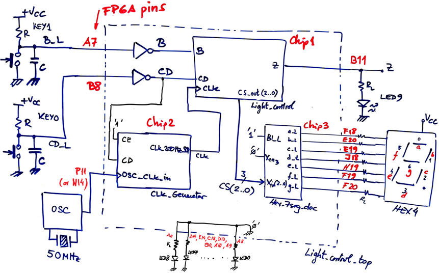
To be able to connect LEDs, buttons and CLK circuits, we have to modify conveniently the circuit as shown in Fig. 18.
|
|
|
Fig. 18. Adapting the Light_Control to the DE10-Lite board. Unused LED will be switch off. A new project Light_Control_top includes the additional blocks for interfacing the hardware. |
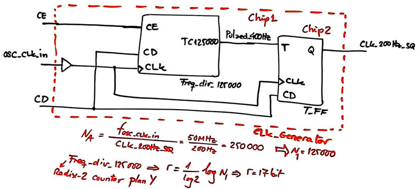
In Chapter 2 projects we have to generate the CLK signal from the external crystal oscillator (Chip2). Particularly in this example the mission of the CLK_generator subsystem, one of the objectives in P8, is to generate a 200 Hz squared CLK signal from the 50 MHz oscillator circuit available in DE10-Lite board. Indeed, the board's crystal oscillator is 24 MH, and it is connected to a CLK chip that generates the 50 MHz signal for the FPGA.
Fig. 19 shown the CLK_Generator.vhd schematic build using two internal components: Freq_div_125000.vhd and T_FF.
|
|
|
Fig. 19. Internal architecture of the CLK_Generator. |
Another convenient debugging tool when prototyping is to be able to watch FSM internal states, for instance current_state using a 7-segment display. We can modify the (Chip1) Light_control.vhd in Fig. 18 to add this extra output CS_out(2..0) connecting it to a Hex_7seg_decoder (Chip3) from Chapter 1.
Translating the top schematic in Fig. 18 as Light_Control_top.vhd we can synthesise the project at the location:
C:\CSD\P6\Light_Control\DE10_Lite\(files)
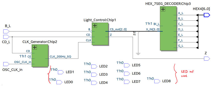
This Light_Control_top is the full (zipped) list of VHDL files to synthesise the board experiment in Fig. 18. The RTL view is represented in Fig. 20.
|
|
Fig. 20. Top RTL circuit including Light_control, CLK_Generator, and Hex_7seg_decoder. |
Pin assignment tool
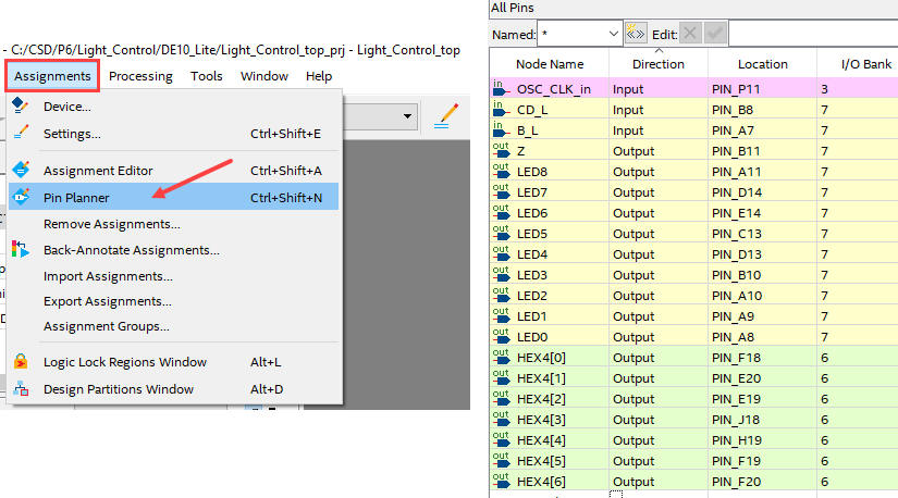
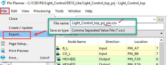
Assign pins using the Pin Planner spreadsheet and generate the output SOF file. The list of pins used can be exported from Pin Planner as Light_Control_top_prj_pins.csv. So that you can as well import this assignment file to your project.
|
a)
b) |
Fig. 21. a) Assigning pins with the pin planner. b) Saving the pin list in csv format. |
Programmer
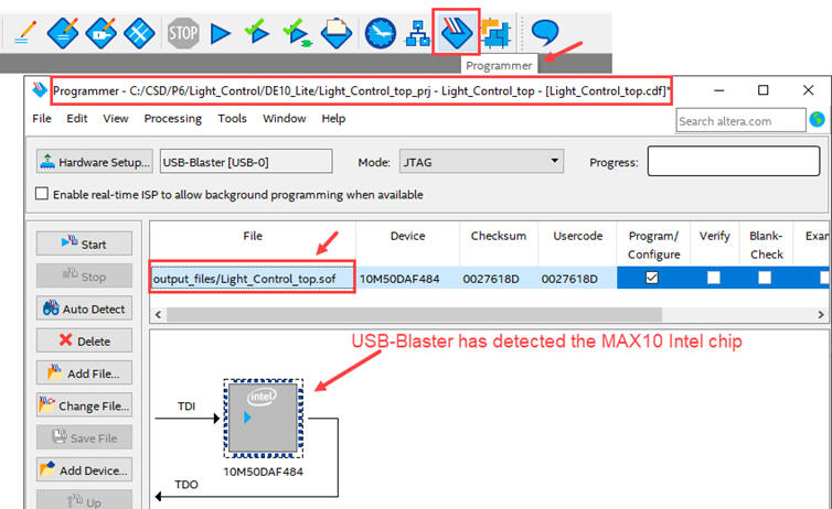
Synthesise and generate the FPGA output configuration Light_Control_top.sof file for the programmer application. Additionally, in case we like to write the configuration flash memory (CFM) of the FPGA and make the circuit permanent (not erased when unplugging the board), the programmer object file (.pof) Light_Control_top.pof is required instead. Remember that the original pof board's configuration file is found here DE10-Lite.
|
|
|
Fig. 22. Once pin are assigned, you can run the programmer. USB-Blaster drivers must be installed. |
Finally, this is a picture of the prototype running the light control application.
|
|
|
Fig. 23. Prototype running. |


